Board connections and settings, Table 2. system connections, Table 3. cdb4353 jumper settings – Cirrus Logic CDB4353 User Manual
Page 6: Table 4. cdb4353 switch settings, Table 4
6
DS803DB2
CDB4353
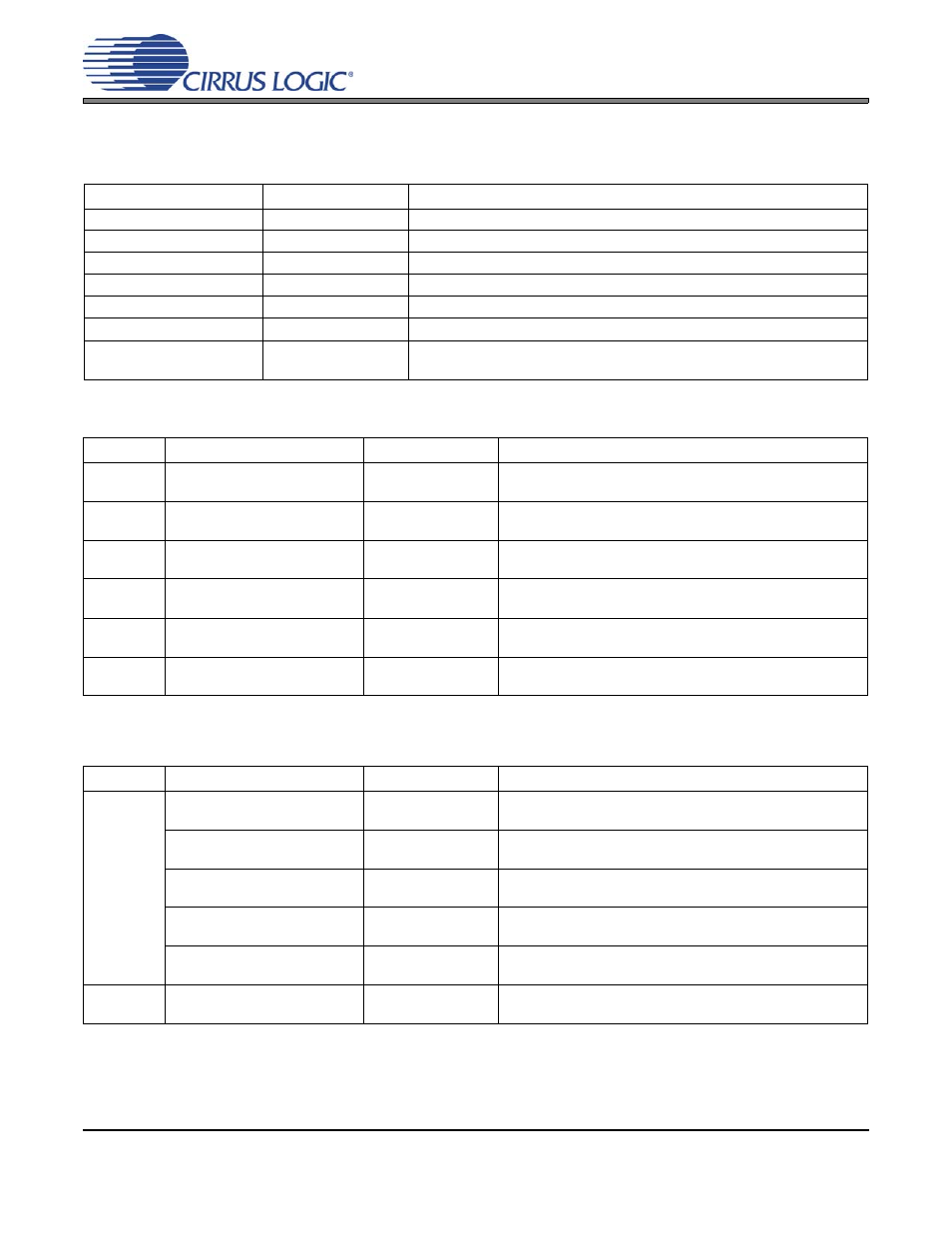
10.BOARD CONNECTIONS AND SETTINGS
Board connections and settings are shown in
,
, and
Table 2. System Connections
Table 3. CDB4353 Jumper Settings
Table 4. CDB4353 Switch Settings
Note:
All settings denoted by an asterisk (*) are the Default Factory Settings.
CONNECTOR
INPUT/OUTPUT
SIGNAL PRESENT
3.3 V - J3
Input
+3.3 V power for the evaluation board
GND - J2
Input
Ground connection from power supply
SPDIF INPUT - J16
Input
Digital audio interface input via coaxial cable
SPDIF INPUT - OPT1
Input
Digital audio interface input via optical cable
PCM INPUT - J13
Input
Input for master, serial, left/right clocks and serial data
EXT SYS CONN - J4
Input
Input for master, serial, left/right clocks and serial data - direct to CS4353
AOUTA - J14
AOUTB - J15
Output
RCA line-level analog outputs
JUMPER
PURPOSE
POSITION
FUNCTION SELECTED
J1
Selects source of voltage for
the VL supply
*shunted
not shunted
Voltage source is +3.3 V binding post (J3)
Voltage source is pin 2 of J1
J8
Current measure for VCP
*shunted
When shunt is removed, the voltage can be measured
across a fixed resistance to determine current.
J9
Current measure for VL
*shunted
When shunt is removed, the voltage can be measured
across a fixed resistance to determine current.
J10
Current measure for VA
*shunted
When shunt is removed, the voltage can be measured
across a fixed resistance to determine current.
J5
CS4353 Reset Select
*EXTERNAL
POR
CS4353 reset by S2
CS4353 uses internal power-on reset
J11
CS4353 Output Reference
*shunted
not shunted
Output reference is board ground
Output reference is J14 and J15 ground
SWITCH
PURPOSE
POSITION
FUNCTION SELECTED
S1
Selects PCM source for
CS4353
1
down = PCM Header J3
*up = CS8416
CS8416 MCLK/LRCK Ratio
2
*down = MCLK is 256xFs
up = MCLK is 128xFs
CS8416 and CS4353 PCM
Format
3
*down = I
2
S
up = LJ
CS4353 Output Amplitude
4
down = 1 V
rms
output
*up = 2 V
rms
output
CS4353 De-emphasis select
5
*down = De-emphasis off
up = De-emphasis on
S2
Resets CS4353 and CS8416
-
CS8416 must be reset if switch S1 position 2 or 3 is
changed