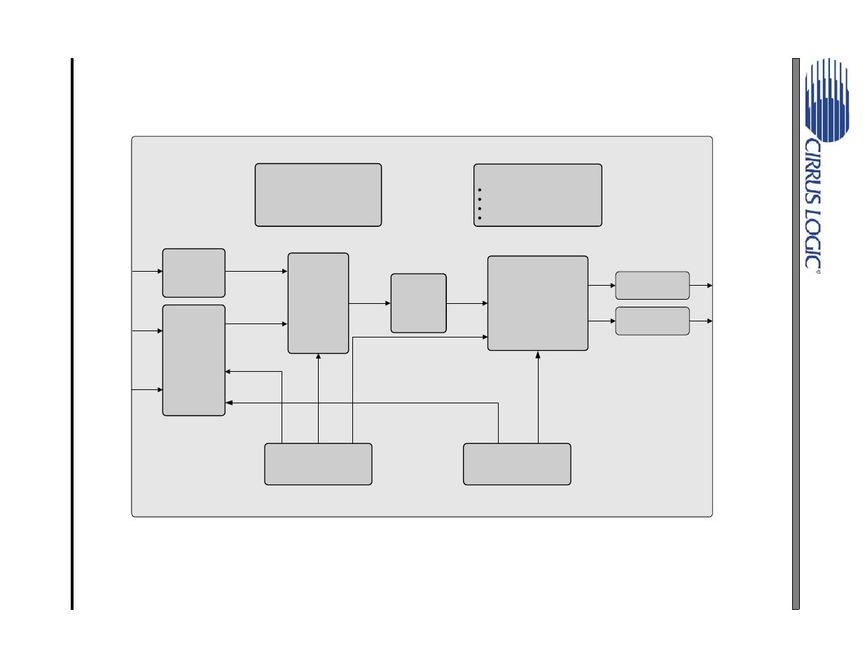
Schematics and layout, Figure 31. system block diagram and signal flow, Figure 31 – Cirrus Logic CDB4353 User Manual
Page 12: Cs4353, Figure 33
12
DS80
3DB2
CDB4353
12.SCHEMATICS AND LAYOUT
Indicator LEDs
S/PDIF Error
S/PDIF or PCM Input Selected
+3.3V power
VL power
CS4353
CS8416
S/PDIF
Receiver
PCM Mux
and Level
Shifter
PCM Clocks/Data
PCM Clocks/Data
CS4353 Settings
PCM
so
urc
e
se
le
ct
CS8416 serial port
format
Analog Outputs
Hardware Control
Switches
Reset Circuit
C
S
4353
Rese
t
CS8416 Reset
External
System
Connector
PCM Clocks/Data
PCM Clocks/Data
PCM Input
Optical
S/PDIF
Input
AOUTA
AOUTB
PCM HEADER
Coaxial
S/PDIF
Input
+3.3V Power
(Optional separate VL)
Figure 31. System Block Diagram and Signal Flow
See also other documents in the category Cirrus Logic Hardware:
- CobraNet (147 pages)
- CS4961xx (54 pages)
- CS150x (8 pages)
- CS1501 (16 pages)
- CS1601 (2 pages)
- CS1601 (16 pages)
- CS1610 (16 pages)
- CRD1610-8W (24 pages)
- CRD1611-8W (25 pages)
- CDB1610-8W (21 pages)
- CS1610A (18 pages)
- CDB1611-8W (21 pages)
- CDB1610A-8W (21 pages)
- CDB1611A-8W (21 pages)
- CRD1610A-8W (24 pages)
- CRD1611A-8W (25 pages)
- CS1615 (16 pages)
- AN403 (15 pages)
- AN401 (14 pages)
- AN400 (15 pages)
- AN375 (27 pages)
- AN376 (9 pages)
- CRD1615-8W (22 pages)
- CRD1616-8W (23 pages)
- AN402 (14 pages)
- AN404 (15 pages)
- CRD1615A-8W (21 pages)
- CS1615A (16 pages)
- CS1630 (56 pages)
- AN374 (35 pages)
- AN368 (80 pages)
- CRD1630-10W (24 pages)
- CRD1631-10W (25 pages)
- CS1680 (16 pages)
- AN405 (13 pages)
- AN379 (31 pages)
- CRD1680-7W (31 pages)
- AN335 (10 pages)
- AN334 (6 pages)
- AN312 (14 pages)
- AN Integrating CobraNet into Audio Products (16 pages)
- CobraNet Audio Routing Primer (9 pages)
- Bundle Assignments in CobraNet Systems (3 pages)
- CS2300-01 (3 pages)
- CS2000-CP (38 pages)