Cirrus Logic CDB4353 User Manual
Cdb4353, Evaluation board for the cs4353, Features
Copyright
© Cirrus Logic, Inc. 2008
(All Rights Reserved)
Evaluation Board for the CS4353
Features
Demonstrates Recommended Layout and
Grounding Arrangements
CS8416 Receives S/PDIF, & EIAJ-340-
Compatible Digital Audio
Headers for External PCM Audio
Single-ended Stereo Analog Outputs
Requires Only a Digital Signal Source and a
+3.3 V Power Supply for a Complete Digital-to-
Analog Converter System
Configured by On-board Hardware Controls
Power, Digital Source Select, and S/PDIF Error
Indicator LEDs
Current Sense Resistors for CS4353 Supplies
(VA, VL, and VCP)
Description
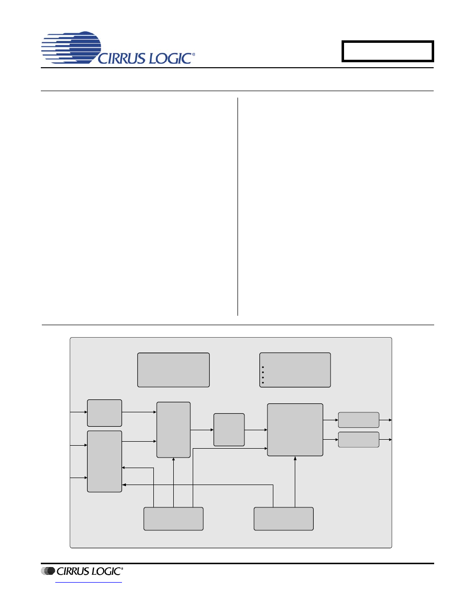
The CDB4353 evaluation board is an excellent means
for quickly evaluating the CS4353 24-bit, high-perfor-
mance stereo D/A converter. Evaluation requires an
analog signal analyzer, a digital signal source, and a
+3.3 V power supply. Analog line-level outputs are pro-
vided via RCA phono jacks.
The CS8416 digital audio receiver IC provides the sys-
tem timing necessary to operate the Digital-to-Analog
converter and will accept S/PDIF and EIAJ-340-com-
patible audio data. The evaluation board may also be
configured to accept external timing and data signals for
operation in a user application during system
development.
The CDB4353 is controlled by switches to select the
digital signal source and configuration options for the
CS4353. Current sense resistors allow for easy power
calculations during system development.
ORDERING INFORMATION
CDB4353
Evaluation Board
Indicator LEDs
S/PDIF Error
S/PDIF or PCM Input Selected
+3.3V power
VL power
CS4353
CS8416
S/PDIF
Receiver
PCM Mux
and Level
Shifter
PCM Clocks/Data
PCM Clocks/Data
CS4353 Settings
PCM
sou
rce
s
e
le
c
t
CS8416 serial port
format
Analog Outputs
Hardware Control
Switches
Reset Circuit
CS
43
53
R
e
se
t
CS8416 Reset
External
System
Connector
PCM Clocks/Data
PCM Clocks/Data
PCM Input
Optical
S/PDIF
Input
AOUTA
AOUTB
PCM Header
Coaxial
S/PDIF
Input
+3.3V Power
(Optional separate VL)
AUG '08
DS803DB2
CDB4353
Document Outline
- Table of Contents
- List of Figures
- List of Tables
- 1. CDB4353 System Overview
- 2. CS4353 Digital-to-Analog Converter
- 3. CS8416 Digital Audio Receiver
- 4. Input for Clocks and Data
- 5. Power Supply Circuitry
- 6. Grounding and Power Supply Decoupling
- 7. Hardware Control
- 8. CS8416 and CS4353 Reset
- 9. Analog Output Filtering
- 10. Board Connections and Settings
- 11. Performance Plots
- Figure 1. FFT (48 kHz, 0 dB)
- Figure 2. FFT (48 kHz, -60 dB)
- Figure 3. FFT (48 kHz, No Input)
- Figure 4. FFT (48 kHz Out-of-Band, No Input)
- Figure 5. 48 kHz, THD+N vs. Input Freq
- Figure 6. 48 kHz, THD+N vs. Level
- Figure 7. 48 kHz, Fade-to-Noise Linearity
- Figure 8. 48 kHz, Frequency Response
- Figure 9. 48 kHz, Crosstalk
- Figure 10. 48 kHz, Impulse Response
- Figure 11. FFT (96 kHz, 0 dB)
- Figure 12. FFT (96 kHz, -60 dB)
- Figure 13. FFT (96 kHz, No Input)
- Figure 14. FFT (96 kHz Out-of-Band, No Input)
- Figure 15. 96 kHz, THD+N vs. Input Freq
- Figure 16. 96 kHz, THD+N vs. Level
- Figure 17. 96 kHz, Fade-to-Noise Linearity
- Figure 18. 96 kHz, Frequency Response
- Figure 19. 96 kHz, Crosstalk
- Figure 20. 96 kHz, Impulse Response
- Figure 21. FFT (192 kHz, 0 dB)
- Figure 22. FFT (192 kHz, -60 dB)
- Figure 23. FFT (192 kHz, No Input)
- Figure 24. FFT (192 kHz Out-of-Band, No Input)
- Figure 25. 192 kHz, THD+N vs. Input Freq
- Figure 26. 192 kHz, THD+N vs. Level
- Figure 27. 192 kHz, Fade-to-Noise Linearity
- Figure 28. 192 kHz, Frequency Response
- Figure 29. 192 kHz, Crosstalk
- Figure 30. 192 kHz, Impulse Response
- 12. Schematics and Layout
- 13. Revision History