Design note, Cdb4351 revision a.0, Cdb4351 revision b.0 – Cirrus Logic CDB4351 User Manual
Page 5: Cdb4351
CDB4351
DS566DB3
5
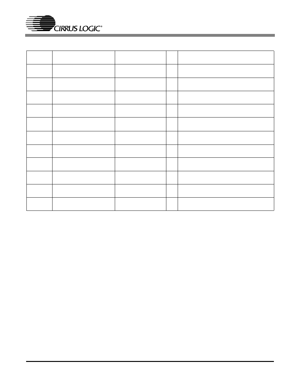
Table 2. CDB4351 Jumper Settings
*Default Factory Settings.
The S/C column denotes standard jumper settings for either stand-alone (S) or control port (C) operation.
8. DESIGN NOTE
CDB4351 Revision A.0
The FET muting circuit must be bypassed by placing a shunt on J13 and J21, otherwise unwant-
ed noise will occur while muted.
CDB4351 Revision B.0
There are no known issues on this revision.
JUMPER /
SWITCH
PURPOSE
POSITION
S/C
FUNCTION SELECTED
J5
Selects source of voltage
for the +5V supplies
+5 V
*+5V_REG
Voltage source is +5 V binding post
Voltage source is +5 V regulator
J6
Selects source of voltage
for the VD supplies
VD
*+3.3V REG
Voltage source is VD binding post
Voltage source is +3.3 V regulator
J7
Selects source of voltage
for the VL supply
VL
*+3.3V REG
Voltage source is VL binding post
Voltage source is +3.3 V regulator
J10
Selects source of voltage
for the VA supply
VA
*+3.3V REG
Voltage source is VA binding post
Voltage source is +3.3 V regulator
S1
Sets Mode of CS8416 and
clock source
*1 = open
*2, 3, 4 = closed
Default setting is I
2
S mode from CS8416
See CS8416 datasheet for details
J20
Stand-alone/Control Port
Select
DIS
*EN
S
C
Stand-alone Mode (No PC required)
Control Port Mode (PC required)
J17
DEM(AD0/CS)
HI
*LO
-
SC
See CS4351 datasheet for details
J18
DIF0(SDA/CDIN)
*HI
LO
C
S
See CS4351 datasheet for details
J19
DIF1(SCL/CCLK)
*HI
LO
C
S
See CS4351 datasheet for details
J15
J24
LOAD select
SHUNTED
*OPEN
Adds resistor for max loading
Normal output circuit
J13
J21
Mute Disable
*SHUNTED
OPEN
Bypasses FET muting
Normal output circuit