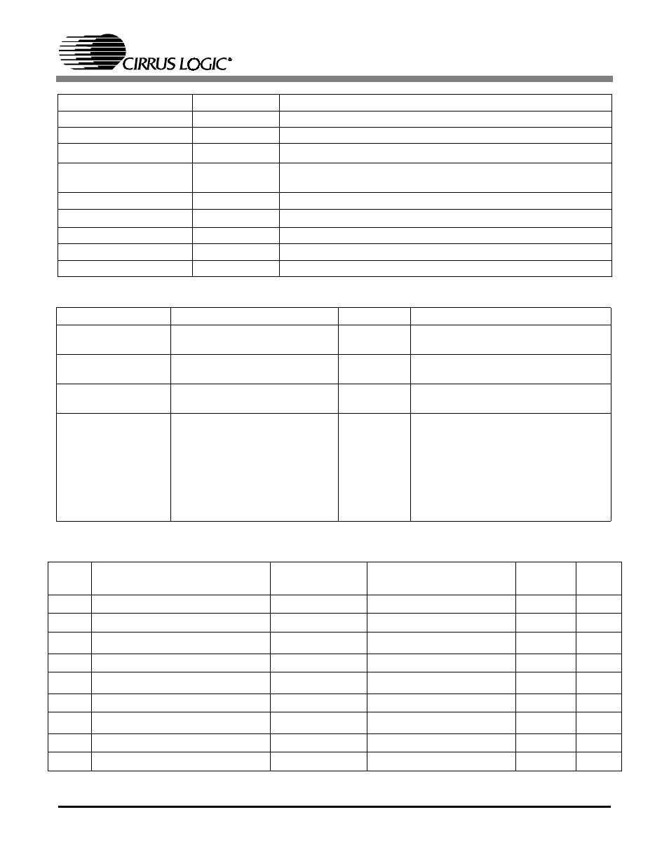
Table 2. jumper settings, 15 external control header signals, Table 3. cs424xx external control header signals – Cirrus Logic CDB42428 User Manual
Page 7
CDB42428
7
1.15
External Control Header Signals
OPT4
Input
CS8416 digital audio interface input via optical
SPDIF TX - J2
Output
CS8406 digital audio interface output via coax
SPDIF TX - OPT2
Output
CS8406 digital audio interface output via optical
PC Port - J22
Input/Output
Parallel connection to computer for SPI / I
2
C control port signals
EXTERNAL CONTROL
HEADER - J17
Input/Output
I/O for SPI / I
2
C control port signals - see signal descriptions below
DSP HEADER - J36
Input/Output
I/O for DSP serial port signals - see signal descriptions below
ANALOG IN LFT/RT
Input
RCA phono jacks for analog input signal to CS424xx internal ADCs
EXT A/D #1 LEFT/RIGHT
Input
RCA phono jacks for analog input signal to CS5361 ADC #1
EXT A/D #2 LEFT/RIGHT
Input
RCA phono jacks for analog input signal to CS5361 ADC #2
OUT_A1 to OUT_B4
Output
RCA phono jacks for channels A1 to B4 analog outputs
JUMPER / SWITCH
PURPOSE
POSITION
FUNCTION SELECTED
J37
Selects source of voltage for the
VLS supplies
+3.3 V
*+5 V
Voltage source is +3.3 V regulator
Voltage source is +5 V binding post
J38
Selects source of voltage for the
VD supply
+3.3 V
*+5 V
Voltage source is +3.3 V regulator
Voltage source is +5 V binding post
S2
Stand-Alone Mode Select
SAM0
SAM1
Stand-Alone Modes are for debug use
and are presently unsupported
J9,J10,J11
J13,J15,J16
J18,J19,J20
J23,J25,J26
J28,J29,J30
J32,J34,J35
J39,J40,J41
J43,J45,J46
DAC Output Filter select - FILT
*1
2
Selects standard 2-pole LPF
Selects instrumentation-amp/LPF/pad
*Default Factory Settings
Table 2. Jumper Settings
Header
Pin #
Signal Description
Source
Schematic Signal Name
Buffer
Buffer
Voltage
1
External Control Present Signal
CTRL
EXT_CONTROL_PRESENT-
-
-
2
Ground
CDB
GND
-
-
3
Address Bit 0 (I
2
C) / CS- (SPI)
CTRL
AD0/CS
74VHC125
VLC
4
Ground
CDB
GND
-
-
5
Address Bit 1 (I
2
C) / CDIN (SPI)
CTRL
AD1/CDIN
74VHC125
VLC
6
Ground
CDB
GND
-
-
7
SDA (I
2
C) / CDOUT (SPI)
CTRL or CS424xx
SDA/CDOUT
MOSFET
VLC
8
Ground
CDB
GND
-
-
9
Serial Control Port Clock
CTRL
SCL/CCLK
74VHC125
VLC
Table 3. CS424xx External Control Header Signals
Table 1. System Connections