Diagrams, Introduction – Agilent Technologies 6613C User Manual
Page 53
53
6
Diagrams
Introduction
This chapter contains drawings and diagrams for troubleshooting and maintaining the Agilent Model
6611C, 6612C, 6613C and 6614C System DC Power Supplies.
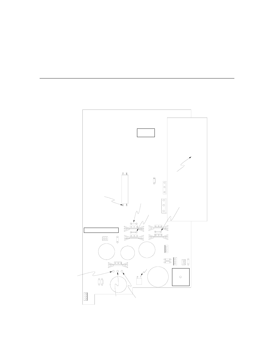
Figure 6-1. A1 Board Component and Test Point Locations
S
e
c
C
o
mmo
n
-Ra
il
+Ra
il
J307
+
15Vs
-15Vs
+5
V
s
F310
R4
3
1
D3
0
7
D3
3
0
+5Vp (unreg)
Pri Common
F3
1
1
F308
F30
5
F30
3
F3
06
J
305
J
304
J3
14
J306
J3
03
F30
9
H
eat
S
in
k
Conductor Side
J320
Rel
a
y
Op
t
Gr
n
/Y
e
l
Ye
llo
w
O
ran
ge
Red
Br
o
w
n
Wh
it
e
Gr
a
y
Vi
ol
et
Bl
u
e
Non
e
+5Vp