Block diagram, Figure 2-3. functional block diagram – Ampro Corporation XTX 820 User Manual
Page 16
Chapter 2
Product Overview
10
Reference Manual
XTX 820
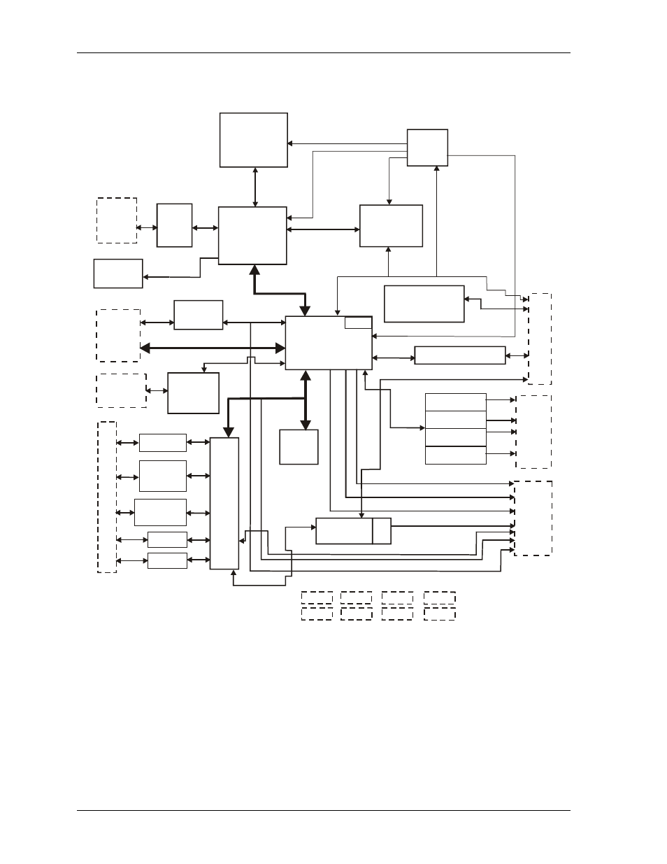
Block Diagram
Figure 2-3 shows the functional components of the board.
XTX820BlkDiagm_a
DDR2
SODIMM
Socket
I/O Hub
82801FBM
(Southbridge)
Memory Bus
Ethernet
PHY
82562
SMBus
Memory &
Graphics Hub
82915GM
(Northbridge)
CRT,
LVDS,
TV Out
PCI Bus
1x IDE Primary
USB Port 3
USB Port 2
USB Port 1
USB Port 0
USB
ATA
Clock
FWH
BIOS
J2(
X
2
)
J4(
X
4
)
J4(X4)
J1(
X
1
)
J3(X3)
J1(X1)
J1 J2 J3 J4
X1 X2 X3 X4
Baseboard Connectors
XTX 820 Connectors
Intel
Pentium M
or Celeron M
CPU
Keyboard,
Mouse
IrDA 1.1
Floppy/
Parallel
COM1
COM2
J3
(X
3
)
Supe
r I
/O
W
8
36
27
H
G
DMI Interface
SDVO
SDVO
LPC Bus
I C
2
Power Ctrl &
Management
2 SATA
USB Ports 4, 5
4 X1 PCI Express Lanes
Board
Controller
WD
T
RTC
Audio
CODEC
SPI
Fan Ctrl
WTD Trig
AC’97/HDA Digital Audio
Figure 2-3. Functional Block Diagram