Dg535 digital delay/pulse generator – Atec Stanford-DG535 User Manual
Page 2
Stanford Research Systems
phone: (408)744-9040
www.thinkSRS.com
In this case, when the A delay is changed, the B output will
move with it. This is useful, for instance, when A and B
specify a pulse and you want the pulse width to remain
constant as the delay of the pulse is changed. Regardless of
how the delay is specified, each delay output will stay asserted
until 800 ns after all delays have timed out. The delays will
then become unasserted, and the unit will be ready to begin a
new timing cycle.
Pulse Outputs
In addition to the four delay outputs, there are four pulse
output channels: AB, –AB, CD and –CD. The leading edge
of the AB pulse coincides with the leading edge of the earlier
of A or B, and the trailing edge of the AB pulse coincides
with the leading edge of the later of B or A. For instance, in
the previous example, a 50 ns pulse would appear at the AB
output and a 1 ms pulse at CD. Pulses as short as 4 ns (FWHM)
can be generated in this manner. The complementary outputs
(–AB and –CD) provide a pulse with identical timing and
inverted amplitude.
Output Amplitude Control
Each delay and pulse output has an independently adjustable
offset and amplitude which can be set between –3 V and +4 V
with 10 mV resolution. The maximum transition for each
output is limited to 4 V. In addition, you can also separately
select 50 Ω or high impedance termination for each output.
Preset levels, corresponding to standard logic families, can
also be selected. TTL, NIM and ECL levels can each be set
with a single key press.
Triggering
The DG535 can be triggered internally from 1 mHz to 1 MHz
with 4-digit frequency resolution. External, single-shot and
burst mode triggers are also supported. For power control
applications, the DG535 can be synchronized to the AC line.
An optional trigger inhibit input allows you to enable or
disable triggering with a TTL level input signal.
±32 Volt Outputs
For applications requiring higher voltages, a rear-panel high
voltage (±32 V) option is available. This option provides five
rear-panel BNCs which output 1 µs pulses at the transition
times of the front-panel T0, A, B, C and D outputs. The high
voltage option does not affect the function or the timing of the
front-panel outputs. The amplitude of the rear-panel outputs
is approximately 8× the corresponding front-panel output,
and the outputs are designed to drive 50 Ω loads. Since they
can only drive an average current of 0.8 mA, charging and
discharging the cable capacitance may be the most important
DG535 Digital Delay/Pulse Generator
TRIG
T0
A
B
C
D
AB
AB
CD
CD
t
TRIG
t
ID
t
A
t
B
t
C
t
D
t
CYCLE
t
BUSY
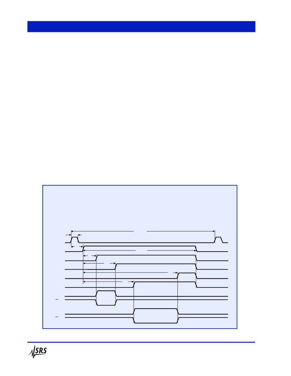
A timing cycle is initiated by an internal or external trig-
ger. T0 is asserted approx. 85 ns after an external trigger.
Outputs A, B, C and D are asserted relative to T0 after
their programmed delays. All of the outputs return low
about 800 ns after the longest delay. The pulse outputs,
AB and CD, go high for the time interval between their
corresponding delay channels.
t
trig
>5 ns
t
cycle
>1 µs + longest delay
t
ID
<85 ns
t
BUSY
<800 ns + longest delay
t
A,B,C,D
0 to 999.999 999 999 995 s
DG535 timing diagram