Pam8615, Pin descriptions – Diodes PAM8615 User Manual
Page 3
PAM8615
Document number: DSxxxxx Rev. 1 - 1
3 of 14
www.diodes.com
October 2012
© Diodes Incorporated
PAM8615
A Product Line of
Diodes Incorporated
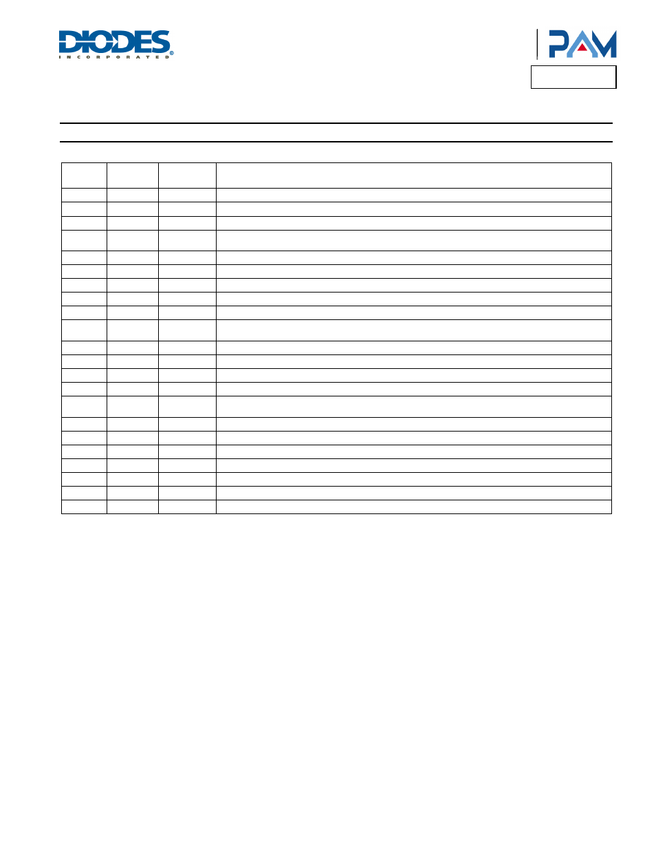
Pin Descriptions
Pin
Number
Pin
Name
I/O/P Function
1 OUT_A O
H-bridge A output.
2 PVCC_A P
Power supply for H-bridge A not connected to PVCC_B or AVCC.
3 SHDN I
Shutdown signal for IC (low = shutdown, high = operat ional). TTL logic levels with compliance to AVCC.
4 MUTE I
Alogic high on this pin disables the outputs. A low on this pin enables the outputs. TTL logic levels with
compliance to AVCC.
5 IN_A I
Audio input for channel A.
6 DGND P
Digital GND
7 IN_B I
Audio input for channel B.
8 VCM O
Reference for analog cells.
9 DCV I
DC voltage setting the gain of the amplifier.
10 MS_SV I
Master/Slave select for determining direction of SYNC terminal. High = Master mode, SYNC terminal is an
output; Low = Slave mode, SYNC terminal accept s a clock input.
11 PVCC_B P
Power supply for H-bridge B, not connected to PVCC_A or AVCC
12, 13
OUT_B
O
H-bridge B output
14 PGND_B P
Power ground for H-bridge B
15 BST_B I/O
Bootstrap I /O for H-bridge B high-side FET
16 VCLAMP P
Internally generated voltage supply for bootst rap. Not to be used as a supply or connected to any component
other than the decoupling capacitor.
17 STNC I/O
Clock i nput/output for synchroni zing multiple class-D devices. Direction determined by MS_SV terminal.
18 AGND P
Analog GND.
19 ROSC I/O
Current s etting resis tor for ramp generator.
20 AVDD P
Analog 5V Regulated output.
21 AVCC P
High-voltage analog power supply.
22 BST_A I/O
Bootstrap I /O for H-bridge A high-side FET.
23 PGND_A P
Power ground for H-bridge A.