Pam8304 new prod uc t, Pin descriptions, Functional block diagram – Diodes PAM8304 User Manual
Page 2: Absolute maximum ratings, Recommended operating conditions
PAM8304
Document number: DS36589 Rev. 1 - 2
2 of 11
October 2013
© Diodes Incorporated
PAM8304
NEW PROD
UC
T
A Product Line of
Diodes Incorporated
Pin Descriptions
Pin Name
MSOP-8L/DFN3x3-8L
Function
OUT+
1
Positive BTL Output
PVDD 2
Power
Supply
VDD
3
Analog Power Supply
IN-
4
Negative Differential Input
IN+
5
Positive Differential Input
/SD
6
Shutdown Terminal, Active Low
GND 7
Ground
OUT- 8
Negative
BTL
Output
Exposed Pad
—
NC
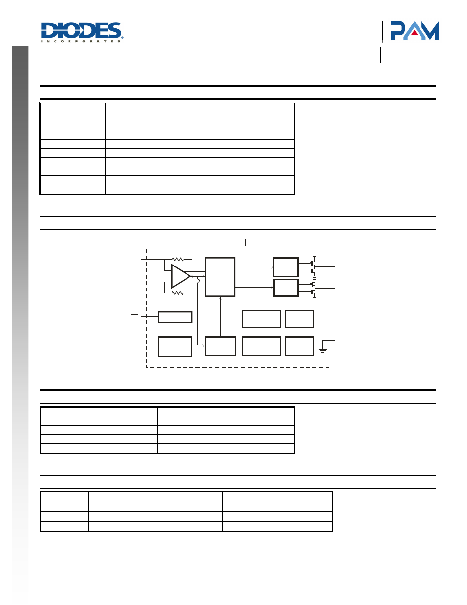
Functional Block Diagram
SD
+
-
PWM
Modulator
SD
UVLO
Startup
Protection
OSC
Bias and
Vref
Gate
Drive
Gate
Drive
SC
Protect
OTP
IN+
IN-
PVDD
OUT+
OUT-
GND
VDD
Absolute Maximum Ratings
(@T
A
= +25°C, unless otherwise specified.)
Parameter Rating
Unit
Supply Voltage (VDD)
6.5
V
Input Voltage (IN+, IN-, /SD)
-0.3 to V
DD
+0.3
V
Storage Temperature
-65 to +150
°C
Maximum Junction Temperature
150
°C
Recommended Operating Conditions
(@T
A
= +25°C, unless otherwise specified.)
Symbol Parameter Min
Max
Unit
V
DD
Supply
Voltage
2.8
6.0
V
T
A
Operating Ambient Temperature Range
-40
+85
°C
T
J
Junction Temperature Range
-40
+125
°C