Pin descriptions, Functional block diagram, Absolute maximum ratings – Diodes PAM8015 User Manual
Page 2: Recommended operating conditions
PAM8013/PAM8015
Document number: DS36979 Rev. 2 - 2
2 of 9
www.diodes.com
May 2014
© Diodes Incorporated
PAM8013/PAM8015
NEW PROD
UC
T
A PRODUCT LINE OF
DIODES INCORPORATED
Pin Descriptions
Pin Name
PAM8013
PAM8015
Function
IN+
A1
A1
Positive differential input
GND A2 B1/B2
Ground
OUT-
A3
A3
Negative BTL output
VDD B1
—
Power
supply
PVDD B2
A2
Power
supply
PGND B3
B3
Power
Ground
IN-
C1
C1
Negative differential input
SD
C2
C2
SD terminal to disable the chip
OUT+
C3
C3
Positive BTL output
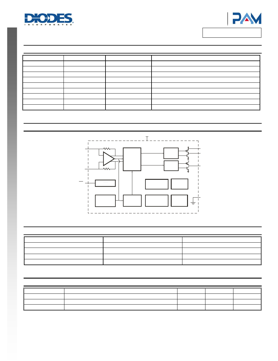
Functional Block Diagram
SD
+
-
PWM
Modulator
SD
UVLO
Startup
Protection
OSC
Bias and
Vref
Gate
Drive
Gate
Drive
SC
Protect
OTP
IN+
IN-
PVDD
OUT+
OUT-
GND
VDD
(PAM8013)
Absolute Maximum Ratings
(@T
A
= +25°C, unless otherwise specified.)
Parameter Rating
Unit
Supply Voltage (VDD)
6.0
V
Input Voltage(IN+, IN-, SD)
-0.3 to V
DD
+0.3
V
Storage Temperature
-65 to +150
°C
Maximum Junction Temperature
150
°C
Recommended Operating Conditions
(@T
A
= +25°C, unless otherwise specified.)
Symbol Parameter
Min
Max
Unit
V
DD
Supply
Voltage
2.8 5.5
V
T
A
Operating Ambient Temperature Range
-25
85
°C
T
J
Junction
Temperature
-40 +125 °C