Pam8006a, Recommended operating conditions, Thermal information – Diodes PAM8006A User Manual
Page 4: Electrical characteristics
PAM8006A
Document number: DSxxxxx Rev. 1 - 0
4 of 13
April 2013
© Diodes Incorporated
PAM8006A
A Product Line of
Diodes Incorporated
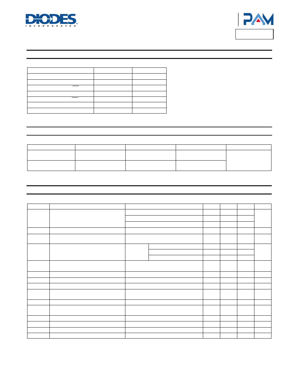
Recommended Operating Conditions
(@T
A
= +25°C, unless otherwise specified.)
Parameter Rating
Unit
Supply Voltage V
CC
8 to 18
V
Input Pin Voltage
0 to 5.5
V
High Level Input Voltage: SD
2.0 to V
CC
V
MUTE
2.0 to 5.5
V
Low Level Input Voltage: SD
0 to 0.3
V
MUTE
0 to 0.3
V
Ambient Operating Temperature
-20 to +85
°C
Thermal Information
Parameter Package Symbol Maximum Unit
Thermal Resisitance
(Junction to Case)
QFN5x5-32L
θ
JC
5.0
°C/W
Thermal Resistance
(Junction to Ambient)
QFN5x5-32L
θ
JA
16.1
The exposed PAD must be soldered to a thermal land on the PCB.
Electrical Characteristics
(@T
A
= +25°C, V
CC
= 12V, R
L
=8Ω, unless otherwise specified.)
Symbol Parameter
Conditions Min
Typ
Max
Units
P
O
Continuous Output Power
THD+N = 0.12%, f = 1kHz, R
L
= 8Ω
6
W
THD+N = 1%, f = 1kHz, R
L
= 8Ω
8.5
THD+N = 10%, f = 1kHz, R
L
= 8Ω
10
I
DD
Quiescent Current
(No Load)
16.5
25
mA
I
SD
Supply Quiescent Current in Shutdown
Mode
Shutdown = 0V
4
10
µA
R
DS(ON)
Drain-Source On-State Resisitance
I
O
= 0.5A
T
J
= +25°C
High Side
210
mΩ
Low Side
210
Total
420
PSRR
Power Supply Ripple Rejection Ratio
1V
PP
Ripple, f = 1kHz,
Inputs AC-Coupled to Ground
-65 dB
f
OSC
Oscillator frequency
300
kHz
Vn
Output Integrated Noise Floor
20Hz to 22kHz, A-Weighting
-100
dB
CS Crosstalk
P
O
= 3W, R
L
= 8Ω, f = 1kHz
-95 dB
SNR
Signal to Noise Ratio
Maximum Output at THD+N < 0.5%,
f = 1kHz
90 dB
Gain
32 dB
|V
OS
|
Output Offset Voltage
(measured differentially)
INN and INP Connected Together
30
mV
V2P5
2.5V Bias Voltage
No Load
2.5
V
AVDD
Internal Analog Supply Voltage
V
CC
= 8V to 26V
5
5.5
V
OTS
Over Temperature Shutdown
160
°C
OTH Thermal
Hysteresis
50
°C