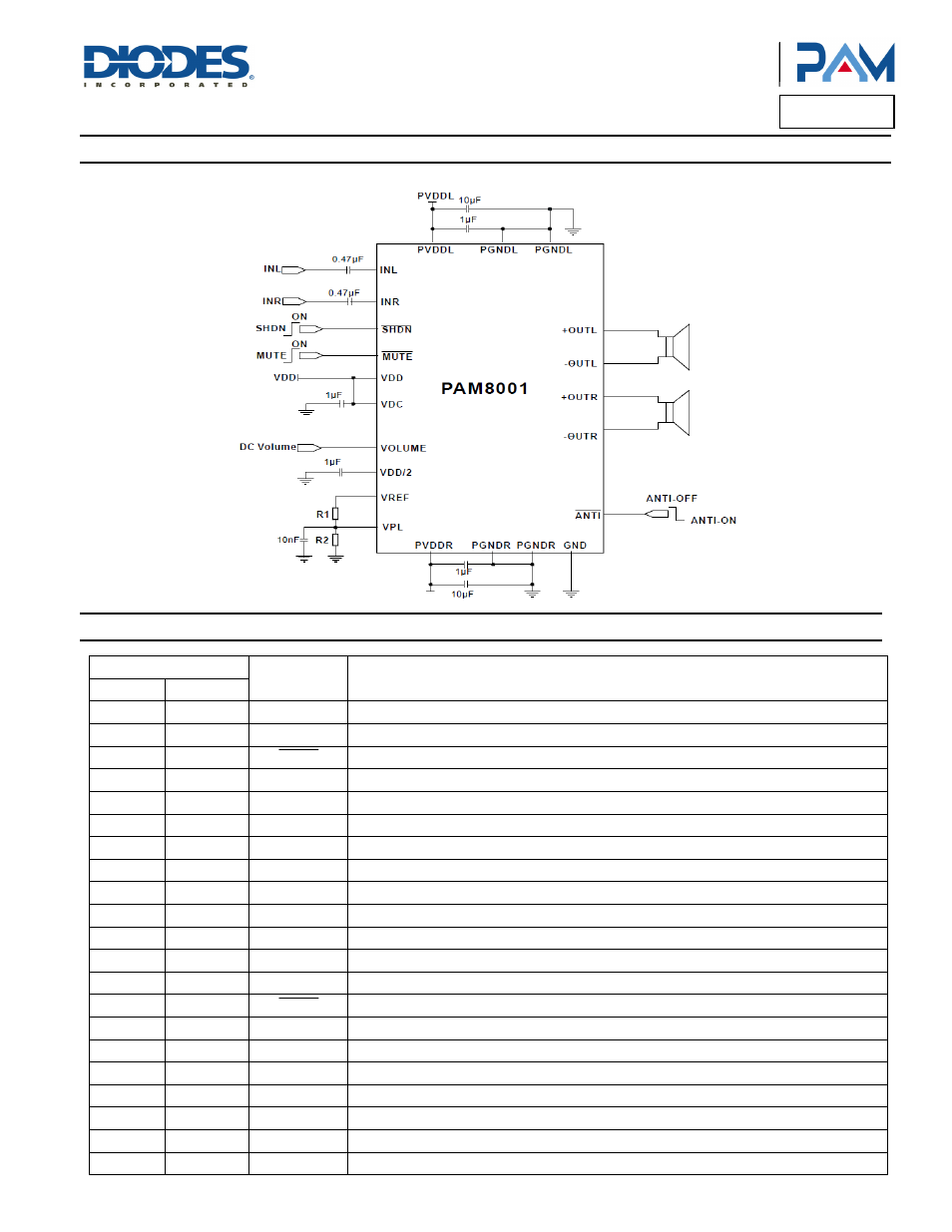
Pam8001, Typical applications circuit, Pin descriptions – Diodes PAM8001 User Manual
Page 2

PAM8001
Document number: DSxxxxx Rev. 1 - 0
2 of 17
February 2013
© Diodes Incorporated
PAM8001
A Product Line of
Diodes Incorporated
Typical Applications Circuit
Pin Descriptions
Pin Number
Pin
Name
Function
QFN3x3 SSOP
1
4
-OUT_L
Left Channel Negative Output
2
5
PVDDL
Left Channel Power Supply
3
6
MUTE
Mute Control Input (active low)
4 7 VDD
Analog
VDD
5
8
INL
Left Channel Input
6
10
VDC
Analog Reference for Gain Control Selection
7
11
VOLUME
DC Volume Control to Set the Gain of Class-D
8 12 ANTI
Anti-Saturation
On/Off
Control
9
14
VDD/2
Internal Common Mode Voltage, Connect a Bypass Capacitior form This Pin to GND
10
15
VPL
Maximum Output Power Setting Voltage
11
16
VREF
Reference Voltage Out for VPL
12
17
INR
Right Channel Input
13 18 GND
Analog
Ground
14
19
SHDN
Shutdown Control Input (active low)
15
20
PVDDR
Right Channel Power Supply
16
21
-OUT_R
Right Channel Negative Output
17
22/23
PGNDR
Right Channel Power GND
18
24
+OUT_R
Right Channel Positive Output
19
1
+OUT_L
Left Channel Positive Output
20
2/3
PGNDL
Left Channel Power GND
9/13 NC
No
Connection
