Pam2805, Pin description, Block diagram – Diodes PAM2805 User Manual
Page 2: Absolute maximum ratings, Recommended operating conditions
PAM2805
Document number: DSxxxxx Rev. 1 - 0
2 of 9
July 2013
© Diodes Incorporated
PAM2805
A Product Line of
Diodes Incorporated
Pin Description
Pin
Number
Pin
Name
Function
1
VIN Input
Voltage
2
GND Power
Ground
3
BLK
Connect A 1µF CAP for blinking
4
FB Feedback
5 VOUT
Output
Voltage
6
SW
Connected to an internal NMOS switch
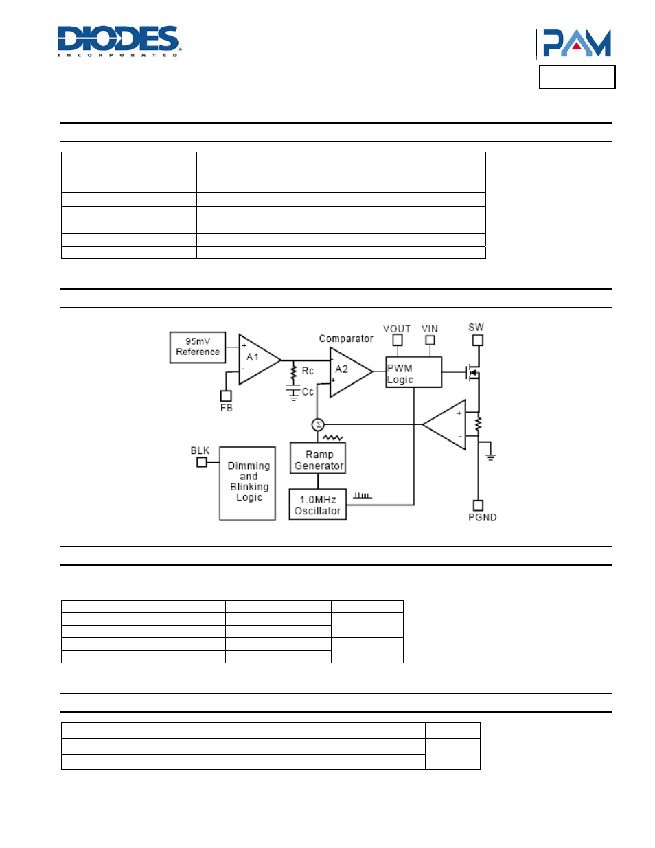
Block Diagram
Absolute Maximum Ratings
(@T
A
= +25°C, unless otherwise specified.)
These are stress ratings only and functional operation is not implied. Exposure to absolute maximum ratings for prolonged time periods may
affect device reliability. All voltages are with respect to ground.
Parameter Rating
Unit
Supply Voltage
6
V
Output Voltage
6
Storage Temperature Range
-65 to +150
°C
Lead Temperature (Soldering, 5 sec)
300
Recommended Operating Conditions
(@T
A
= +25°C, unless otherwise specified.)
Parameter Rating
Unit
Operation Temperature Range
-40 to +85
°C
Junction Temperature Range
-40 to +125