Pam2319, Application information, Ordering information – Diodes PAM2319 User Manual
Page 10

PAM2319
Document number: DSxxxxx Rev. 1 - 1
10 of 12
www.diodes.com
November 2012
© Diodes Incorporated
PAM2319
A Product Line of
Diodes Incorporated
Application Information
(cont.)
Short Circuit Protection
Channel 1:
The swich peak current is limited cycle-by-cycle to a typical vaule in the event of an output voltage short circuit. The device operates with a
frequency of 1MHz and minimum duty clycle. Therefore the average input current is typical 350mA (V
IN
= 3.3V).
Channel 2:
When the converter output is shorted or the device is overloaded, each high-side MOSFET current-limit event (3A typ) turns off the high-side
MOSFET and turns on the low-side MOSFET. An internal counter is used to count the each current-limit event. The counter is reset after
consecutive high-side MOSFETs turn on without reaching current limit. If the current-limit condition persists, the counter fills up. The control logic
then stops both high-side and lowside MOSFETs and waits for a hiccup period, before attemping a new soft-start sequence. The counter bits is
decided by V
FB
voltage. If V
FB
0 2, the counter is 3-bit counter; if VFB > 0.2 the counter is 6-bit counter. The typical hicuup made duty cycle is
1.7%. The hiccup mode is disable during soft-start time.
PCB Layout Check List
When laying out the printed circuit board, the following checklist should be used to ensure proper operation of the PAM2319. Check the following
in your layout:
1. The input capacitor should be close to IC as close as possible.
2. Minimize the switching loop area to avoid excessive switching noise.
3. Two parts GND should be separately layout to avoid disturbing by each other.
4. Must put a small decoupling capacitor between Vin2 Pin and AGND2 Pin.
5. Vo2 output capacitor should be close to output connector to minimize PCB t race resistance affect on ripple voltage. Recommend use two
output capacitor, one close to inductor and IC, another close to output connector.
6. PGND1 Pin should not directly connect to the thermal pad (PGND), it should connect to input capacitor GND then to other GND.
7. AGND should connect to PGND at input capacitor GND.
8. For the good thermal dissipation, PAM2316 has a heat dissipate pad in the bottom side, it should be soldered to PCB surface. For the copper
area can't be large in the component side, so we can use multiple vias connect to other side of the PCB.
9. Avoid using vias in the high-current paths. If vias are unavoidable, use multiple vias in parallel to reduce resistance and inductance.
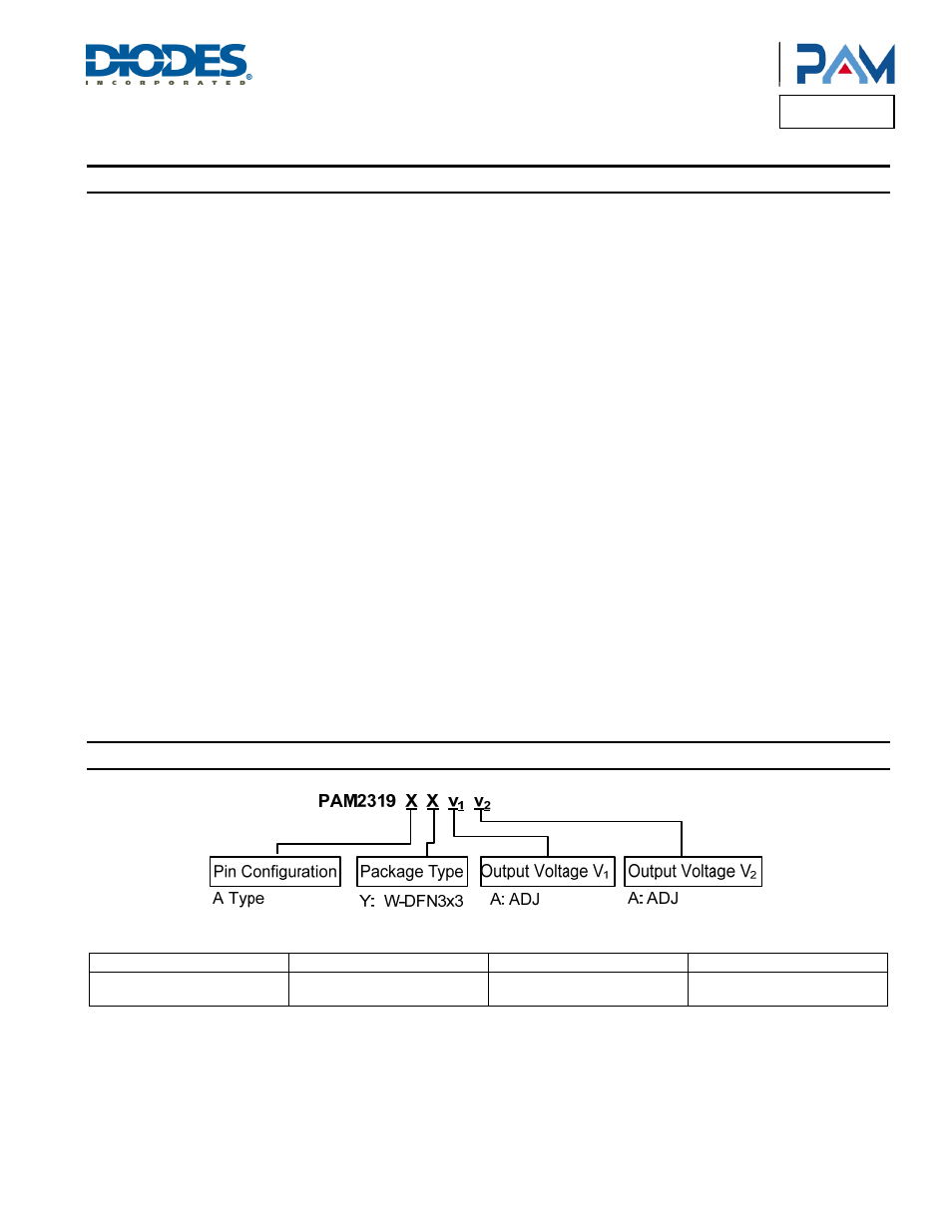
Ordering Information
Part Number
Part Marking
Package Type
Standard Package
PAM2319AYAA
BNAA
XXXYW
W-DFN3x3-12L
3000 Units/Tape & Reel
