Pam2304, Application information, Ordering information – Diodes PAM2304 User Manual
Page 10: Marking information
PAM2304
Document number: DSxxxxx Rev. 1 - 1
10 of 14
www.diodes.com
November 2012
© Diodes Incorporated
PAM2304
A Product Line of
Diodes Incorporated
Application Information
(cont.)
PCB Layout Check List
When laying out the printed circuit board, the following checklist should be used to ensure proper operation of the PAM2304. These items are
also illustrated graphically in Figure 1. Check the following in your layout:
1. The power traces, consisting of the GND trace, the SW trace and the VIN trace should be kept short, direct and wide.
2. Does the V
FB
pin connect directly to the feedback resistors? The resistive divider R1/R2 must be connected between the (+) plate of C
OUT
and
ground.
3. Does the (+) plate of C
IN
connect to V
IN
as closely as possible? This capacitor provides the AC current to the internal power MOSFETs.
4. Keep the switching node, SW, away from the sensitive V
FB
node.
5. Keep the (–) plates of C
IN
and C
OUT
as close as possible.
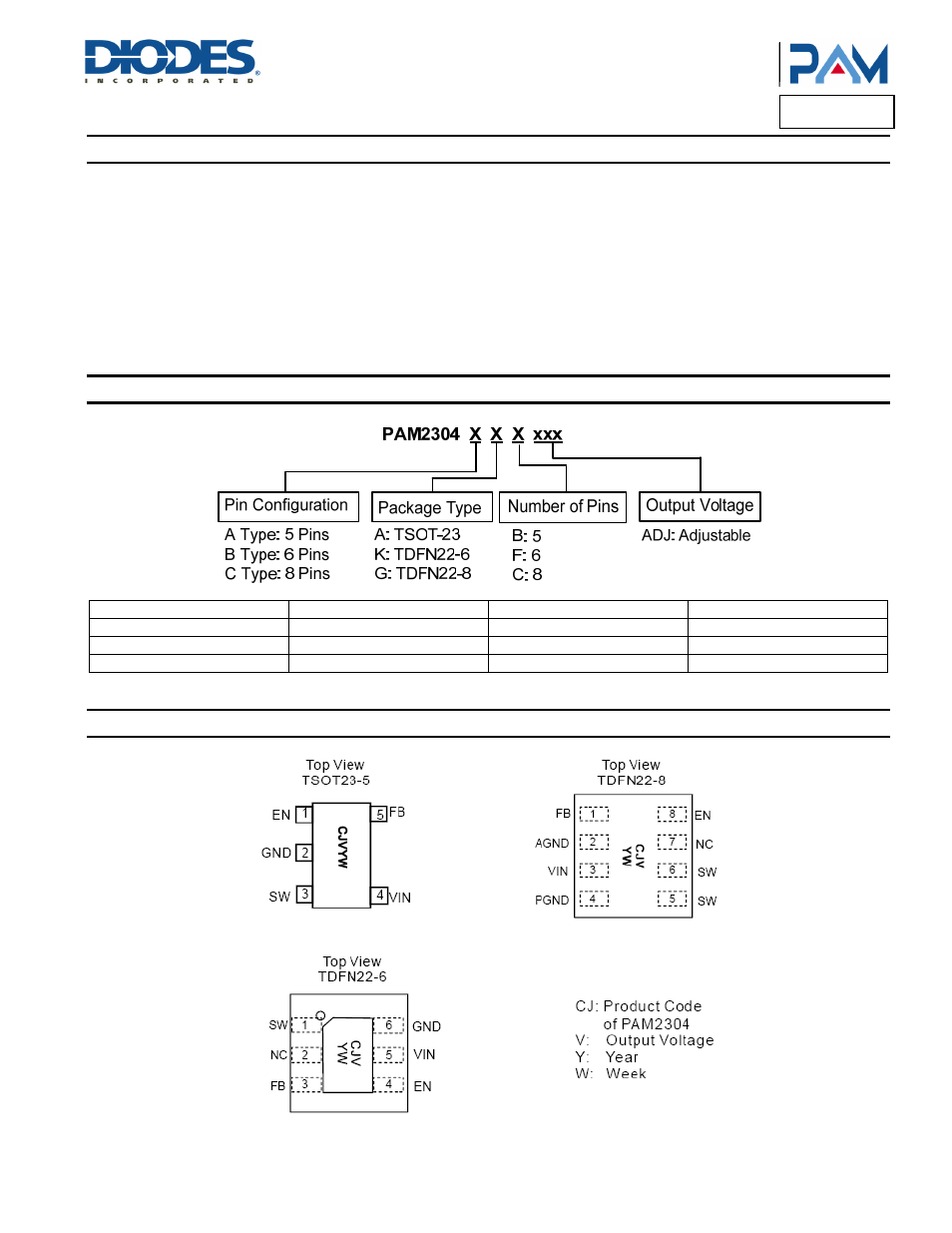
Ordering Information
Part Number
Output Voltage
Package
Packaging
PAM2304AABADJ
ADJ
TSOT23-5
3000 Units/Tape & Reel
PAM2304BKFADJ
ADJ
TDFN22-6
3000 Units/Tape & Reel
PAM2304CGCADJ
ADJ
TDFN22-8
3000 Units/Tape & Reel
Marking Information