Electrical characteristics, Pin functions, A product line of diodes incorporated – Diodes ZXTR1005PD8 User Manual
Page 4
ZXTR1005PD8
Datasheet
Number: DS36316 Rev. 1 - 2
4 of 8
January 2014
© Diodes Incorporated
ZXTR1005PD8
A Product Line of
Diodes Incorporated
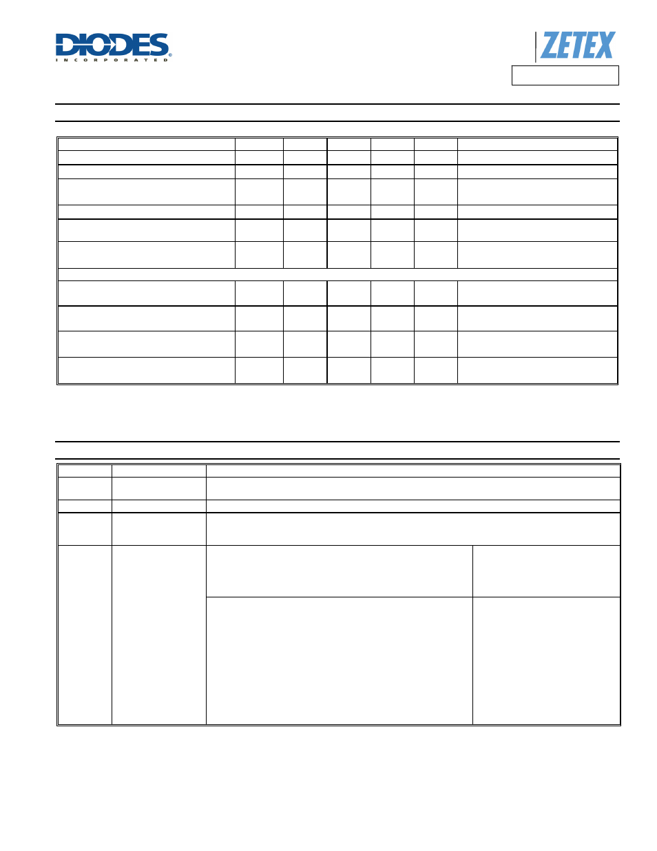
Electrical Characteristics
(Voltage relative to GND, @T
A
= +25°C, unless otherwise specified.)
Enable Output with EN =OPEN (i.e. -100nA < I
EN
< 100nA)
Characteristic Symbol
Min
Typ
Max
Unit
Test
Condition
Output Voltage (Note 12)
V
OUT
4.9 5.0 5.1 V
V
IN
= 48V, I
OUT
= 15mA
Line Regulation (Note 12 & 13)
∆V
OUT
-10 2 10 mV
V
IN
= 10 to 100V, I
OUT
= 15mA
Average Temperature Coefficient
∆V
OUT
/∆T
— 0.44 0.7
mV/°C
T
J
= -55°C to +125°C
V
IN
= 48V, I
OUT
= 15mA
Load Regulation (Note 12 & 14)
∆V
OUT
— 20 50 mV
I
OUT
= 0.1 to 50mA, V
IN
= 48V
Minimum Value of Input Voltage Required to
Maintain Line Regulation
V
IN(MIN)
10 — — V
—
Power Supply Rejection Ratio
ΔV
IN
/
ΔV
OUT
— 57 — dB
C
OUT
= 100nF, I
OUT
= 15mA,
V
OUT
= 5V, V
IN
= 10 to 100V,f = 100Hz
Toggle Output On/Off
Enable Output
V
OUT
4.9 5.0 5.1 V
EN = OPEN, -100nA < I
EN
<100nA,
V
IN
= 48V, I
OUT
= 15mA
Disable Output
V
OUT
— 0 1 V
EN = GND, -0.3V < V
EN
< 1V,
V
IN
= 48V, I
OUT
= 100nA
Quiescent Current (Note 12)
with Enable Output
I
Q
—
300
650
500
900
µA
EN = OPEN, V
IN
= 48V
EN = OPEN, V
IN
= 100V
Quiescent Current (Note 12)
with Disable Output
I
Q
—
300
650
500
900
µA
EN = GND, V
IN
= 48V
EN = GND, V
IN
= 100V
Notes:
12. Measured under pulsed conditions. Pulse width ≤ 300μs. Duty cycle ≤ 2%.
13. Line regulation
ΔV
OUT
= V
OUT
(@ V
IN
= 100V) – V
OUT
(@ V
IN
= 10V)
14. Load regulation
ΔV
OUT
= V
OUT
(@ I
OUT
= 50mA) – V
OUT
(@ I
OUT
= 0mA)
Pin Functions
Pin Name
Pin Function
Notes
V
IN
Input Supply
To maintain output regulation the input voltage can vary from 10V to 100V with respect to the GND pin. It is
recommended to connect a 1µF capacitor to GND.
GND
Power Ground
This pin should be tied to the system ground.
V
OUT
Voltage Output
Outputs a regulated 5V when drawing between 0.1 to 50mA current. It is recommended to connect a
≥100nF capacitor to GND to minimize the noise on the regulated output. The pin can be pulled high to a
maximum of 10V with respect to ground.
EN
Enable Output
Output Always On
When the output state is required to be permanently on, then the EN
pin should be left floating in an OPEN state.
EN pin = Do not connect
Toggle Output On/Off
Toggle the regulator’s output state between on (5V) and off (0V).
Enable Output
Leave the EN pin floating in an OPEN state.
Disable Output
Pull the EN pin to GND in a SHORT state.
For example, see the Typical Application Circuit showing a transistor
toggling the EN pin.
Enable Output
EN pin = -100nA < I
EN
<100nA
Disable Output
EN pin = -0.3V < V
EN
< 1V