Diodes ZXTP03200BG User Manual
Page 2
ZXTP03200BG
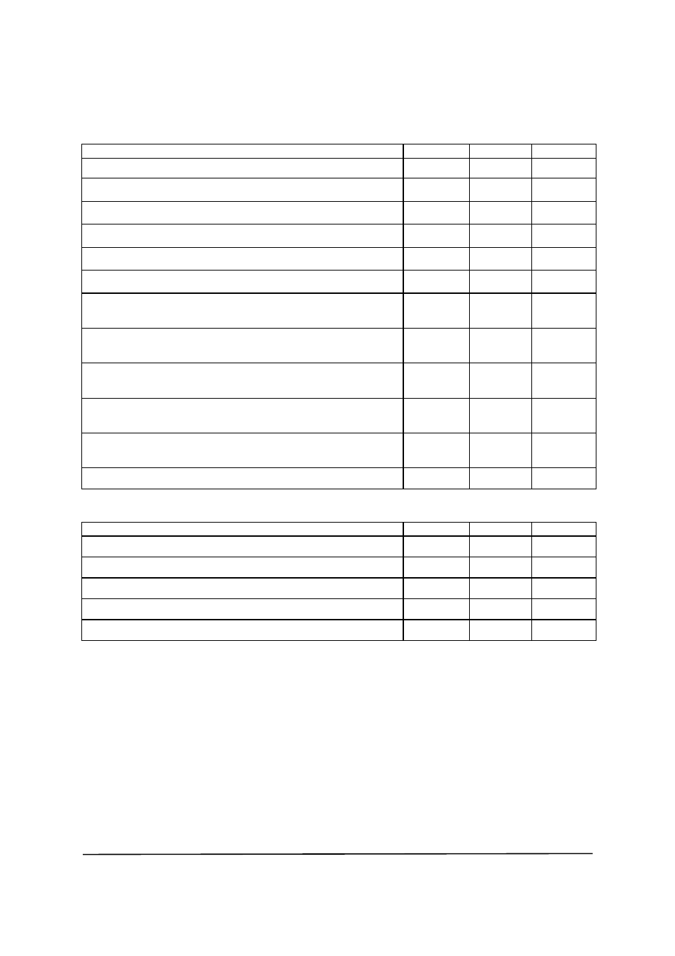
Absolute Maximum Ratings
Parameter Symbol
Limit
Unit
Collector-Base Voltage
V
CBO
-220 V
Collector-Emitter Voltage
V
CEO
-200 V
Emitter-Base Voltage
V
EBO
-7 V
Continuous Collector Current
(a)
I
C
-2 A
Base Current
I
B
-1 A
Peak Pulse Current
I
CM
-5 A
Power Dissipation at T
A
=25
°C
(a)
Linear Derating Factor
P
D
1.25
10
W
mW/
°C
Power Dissipation at T
A
=25
°C
(b)
Linear Derating Factor
P
D
1.65
13.2
W
mW/
°C
Power Dissipation at T
A
=25
°C
(c)
Linear Derating Factor
P
D
3
24
W
mW/
°C
Power Dissipation at T
A
=25
°C
(d)
Linear Derating Factor
P
D
5.8
46.5
W
mW/
°C
Power Dissipation at T
C
=25
°C
(e)
Linear Derating Factor
P
D
11.9
95.2
W
mW/
°C
Operating and Storage Temperature Range
T
j
, T
stg
-55 to 150
°C
Thermal Resistance
Parameter Symbol
Value
Unit
Junction to Ambient
(a)
R
θJA
100
°C/W
Junction to Ambient
(b)
R
θJA
76
°C/W
Junction to Ambient
(c)
R
θJA
41.6
°C/W
Junction to Ambient
(d)
R
θJA
21.5
°C/W
Junction to Lead
(e)
R
θJL
10.5
°C/W
NOTES:
(a)
For a device surface mounted on 15mm x 15mm x 1.6mm FR4 PCB with high coverage of single sided 1oz copper, in still
air conditions.
(b)
Mounted on 25mm x 25mm x 1.6mm FR4 PCB with high coverage of single sided 1oz copper, in still air conditions.
(c)
Mounted on 50mm x 50mm x 1.6mm FR4 PCB with high coverage of single sided 2oz copper, in still air conditions.
(d)
As (c) above measured at t<5 seconds.
(e)
Junction to Lead from Collector Tab.Typical
Issue 1 - August 2008 2
© Diodes Incorporated 2008
www.zetex.com
www.diodes.com