Maximum ratings, Thermal characteristics, A product line of diodes incorporated – Diodes ZXTP25100CFH User Manual
Page 2
ZXTP25100CFH
Document Number: DS33758 Rev. 3 - 2
2 of 7
August 2012
© Diodes Incorporated
A Product Line of
Diodes Incorporated
ZXTP25100CFH
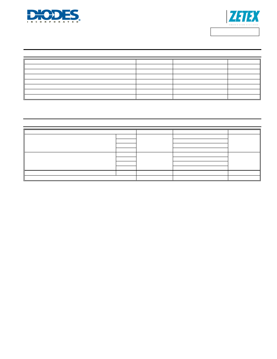
Maximum Ratings
(@T
A
= +25°C, unless otherwise specified.)
Characteristic Symbol
Value
Unit
Collector-Base Voltage
V
CBO
-115 V
Collector-Emitter Voltage
V
CEO
-100 V
Emitter-collector voltage (reverse blocking)
V
ECO
-7 V
Emitter-Base Voltage
V
EBO
-7 V
Continuous Collector Current (Note 5)
I
C
-1 A
Base Current
I
B
-500 mA
Peak Pulse Current
I
CM
-3 A
Thermal Characteristics
(@T
A
= +25°C, unless otherwise specified.)
Characteristic Symbol
Value
Unit
Collector Power Dissipation
(Note 5)
P
D
0.73
W
(Note 6)
1.05
(Note 7)
1.25
(Note 8)
1.81
Thermal Resistance, Junction to Ambient
(Note 5)
R
θJA
171
°C/W
(Note 6)
119
(Note 7)
100
(Note 8)
69
Thermal Resistance, Junction to Leads
(Note 9)
R
θJL
75.25
°C/W
Operating and Storage Temperature Range
T
J,
T
STG
-55 to +150
°C
Notes:
5. For the device mounted on 15mm X 15mm X 1.6mm FR4 PCB with high coverage of single sided 1oz copper in still air condition;
6. Mounted on 25mm X 25mm X 1.6mm FR4 PCB with high coverage of single sided 2oz copper in still air condition
7. Mounted on 25mm X 25mm X 1.6mm FR4 PCB with high coverage of single sided 2oz copper in still air condition
8. As Note 7 above, measured at t < 5 secs.
9. Thermal resistance from junction to solder-point (at the end of the collector lead).