Package outline dimensions, Suggested pad layout, Zxtp2013g – Diodes ZXTP2013G User Manual
Page 6
ZXTP2013G
Da
tasheet Number: DS33714 Rev. 2 - 2
6 of 7
May 2013
© Diodes Incorporated
ZXTP2013G
A Product Line of
Diodes Incorporated
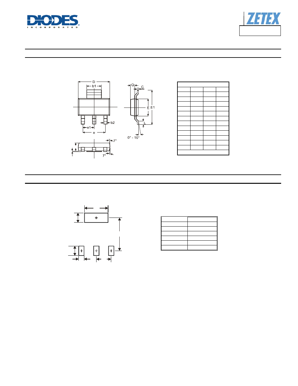
Package Outline Dimensions
Please see AP02002 at latest version.
Suggested Pad Layout
Please see AP02001 at the latest version.
For high voltage applications, the appropriate industry sector guidelines should be considered with regards to creepage and clearance distances between device
terminals and PCB tracking.
SOT223
Dim
Min
Max
Typ
A
1.55
1.65
1.60
A1
0.010 0.15
0.05
b1
2.90
3.10
3.00
b2
0.60
0.80
0.70
C
0.20
0.30
0.25
D
6.45
6.55
6.50
E
3.45
3.55
3.50
E1
6.90
7.10
7.00
e
—
—
4.60
e1
—
—
2.30
L
0.85
1.05
0.95
Q
0.84
0.94
0.89
All Dimensions in mm
Dimensions Value (in mm)
X1
3.3
X2
1.2
Y1
1.6
Y2
1.6
C1
6.4
C2
2.3
A1
A
X2
C1
C2
X1
Y2
Y1
- PDS3200 (5 pages)
- PDS340 (5 pages)
- PDS340Q (5 pages)
- PDS360 (5 pages)
- PDS360Q (5 pages)
- PDS4150 (4 pages)
- PDS3100Q (5 pages)
- PDS3100 (5 pages)
- PDS1240CTL (5 pages)
- PDS1045 (5 pages)
- PDS1040L (5 pages)
- PDS1040CTL (5 pages)
- PDS1040 (5 pages)
- PD3S230L (5 pages)
- PD3S230H (3 pages)
- PDS5100Q (5 pages)
- PDS835L (5 pages)
- PDS760 (5 pages)
- PDS560 (5 pages)
- PDS540 (5 pages)
- PDS5100H (5 pages)
- PDS5100 (5 pages)
- PDS4200H (6 pages)
- SBL3060CTP (4 pages)
- SBL30L30CT (3 pages)
- SBL3045CTP (4 pages)
- SBL3040CTP (4 pages)
- SBL2060CTP (4 pages)
- SBL2030CT - SBL2060CT (3 pages)
- SBL2045CTP (4 pages)
- SBL1060CTP (4 pages)
- SBL1040CTP (4 pages)
- SBG3030CT - SBG3045CT (5 pages)
- SB520 - SB560 (3 pages)
- SB370 - SB3100 (3 pages)
- SB320 - SB360 (3 pages)
- SBR10U100CT (5 pages)
- SBR10U150CT (5 pages)
- SBR10A45SP5 (5 pages)
- SBR1060CT (5 pages)
- SBR1045SP5 (5 pages)
- SBR1045SD1 (4 pages)
- SBR1045D1 (5 pages)
- SBR1045CTL (4 pages)
- SBR1040CT (5 pages)