Absolute maximum ratings, Thermal characteristics, Electrical characteristics – Diodes MMDT2907A User Manual
Page 2: Mmdt2907a
MMDT2907A
Datasheet Number DS30109 Rev.14 - 2
2 of 5
March 2014
© Diodes Incorporated
MMDT2907A
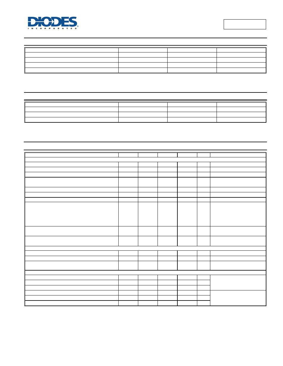
Absolute Maximum Ratings
(@T
A
= +25°C unless otherwise specified.)
Characteristic Symbol
Value
Unit
Collector-Base Voltage
V
CBO
-60 V
Collector-Emitter Voltage
V
CEO
-60 V
Emitter-Base Voltage
V
EBO
-5.0 V
Collector Current
I
C
-600 mA
Thermal Characteristics
(@T
A
= +25°C unless otherwise specified.)
Characteristic Symbol
Value
Unit
Power Dissipation (Note 6)
P
D
200 mW
Thermal Resistance, Junction to Ambient Air (Note 6)
R
θJA
625
C/W
Operating and Storage Temperature Range
T
J
, T
STG
-55 to +150
C
Electrical Characteristics
(@T
A
= +25°C unless otherwise specified.)
Characteristic
Symbol
Min
Typ
Max
Unit Test Condition
OFF CHARACTERISTICS
Collector-Base Breakdown Voltage
BV
CBO
-60 — — V
I
C
= -10µA, I
B
= 0
Collector-Emitter Breakdown Voltage (Note 7)
BV
CEO
-60 — — V
I
C
= -10mA, I
B
= 0
Emitter-Base Breakdown Voltage
BV
EBO
-5 — —
V
I
E
= -10µA, I
C
= 0
Collector Cutoff Current
I
CBO
—
—
—
—
-10
-10
nA
µA
V
CB
= -50V, I
E
= 0
V
CB
= -50V, I
E
= 0, T
A
= +125°C
Collector Cutoff Current
I
CEX
— — -50
nA
V
CE
= -30V, V
EB(OFF)
= -0.5V
Base Cutoff Current
I
BL
— — -50
nA
V
CE
= -30V, V
EB(OFF)
= -0.5V
ON CHARACTERISTICS (Note 7)
DC Current Gain
h
FE
75
100
100
100
50
—
—
—
—
—
—
—
—
300
—
—
I
C
= -100µA ,V
CE
= -10V
I
C
= -1.0mA, V
CE
= -10V
I
C
= -10mA, V
CE
= -10V
I
C
= -150mA, V
CE
= -10V
I
C
= -500mA, V
CE
= -10V
Collector-Emitter Saturation Voltage
V
CE(sat)
— —
-0.4
-1.6
V
I
C
= -150mA, I
B
= -15mA
I
C
= -500mA, I
B
= -50mA
Base-Emitter Saturation Voltage
V
BE(sat)
— —
-1.3
-2.6
V
I
C
= 150mA, I
B
= 15mA
I
C
= 500mA, I
B
= 50mA
SMALL SIGNAL CHARACTERISTICS
Output Capacitance
C
OBO
— — 8.0
pF
V
CB
= -10V, f = 1.0MHz, I
E
= 0
Input Capacitance
C
IBO
— — 30
pF
V
EB
= -2.0V, f = 1.0MHz, I
C
= 0
Current Gain Bandwidth Product
f
T
200 — —
MHz
V
CE
= -20V, I
C
= -50mA,
f = 100MHz
SWITCHING CHARACTERISTICS
Turn-On Time
t
off
— — 45
ns
V
CC
= -30V, I
C
= -150 mA,
I
B1
= -15mA
Delay Time
t
d
— — 10
ns
Rise Time
t
r
— — 40
ns
Turn-Off TIme
t
off
— — 100
ns
V
CC
= -6V, I
C
= -150 mA,
I
B1
= -I
B2
= -15mA
Storage Time
t
s
— — 80
ns
Fall Time
t
f
— — 30
ns
Notes:
6. For the device mounted on minimum recommended pad layout FR4 PCB with high coverage of single sided 1oz copper, in still air conditions; the device
is measured when operating in a steady-state condition.
7. Short duration pulse test used to minimize self-heating effect.