Diodes MMBD5004BRM User Manual
Mmbd5004brm new prod uc t, Features, Mechanical data
MMBD5004BRM
Document number: DS30714 Rev. 4 - 2
1 of 5
www.diodes.com
December 2009
© Diodes Incorporated
MMBD5004BRM
NEW PROD
UC
T
HIGH VOLTAGE SURFACE MOUNT SWITCHING DIODE ARRAY
Features
•
Two Series Diode Circuits Connect to Form Full Wave Bridge
•
Fast Switching Speed
• Low
Capacitance
•
400V Reverse Breakdown Voltage Rating
•
Lead Free/RoHS Compliant Version (Note 3)
•
"Green" Device (Note 4)
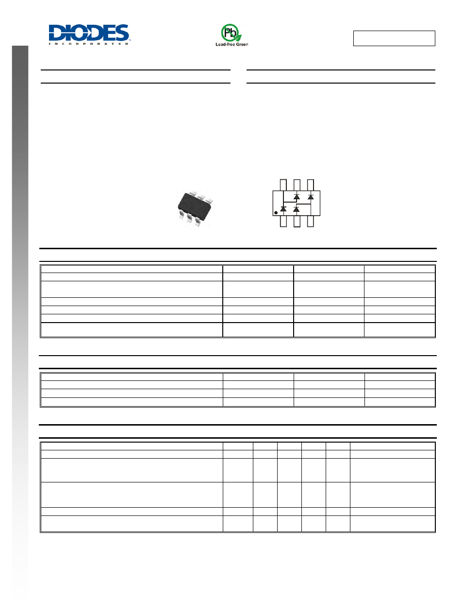
Mechanical Data
• Case:
SOT-26
•
Case Material: Molded Plastic, "Green" Molding Compound,
Note 4. UL Flammability Classification Rating 94V-0
•
Moisture Sensitivity: Level 1 per J-STD-020
•
Terminals: Matte Tin Finish annealed over Copper leadframe
(Lead Free Plating). Solderable per MIL-STD-202, Method 208
•
Polarity: See Diagram
•
Marking Information: See Page 2
•
Ordering Information: See Page 2
•
Weight: 0.016 grams (approximate)
Maximum Ratings
@T
A
= 25°C unless otherwise specified
Characteristic Symbol
Value
Unit
Repetitive Peak Reverse Voltage
V
RRM
400 V
Working Peak Reverse Voltage
DC Blocking Voltage
V
RWM
V
R
350 V
RMS Reverse Voltage
V
R(RMS)
247 V
Forward Continuous Current
I
F
225 mA
Peak Repetitive Forward Current
I
FRM
625 mA
Non-Repetitive Peak Forward Surge Current
@ t = 1.0ms
@ t = 1.0s
I
FSM
2.0
1.0
A
Thermal Characteristics
Characteristic Symbol
Value
Unit
Power Dissipation (Note 1)
P
D
350 mW
Thermal Resistance Junction to Ambient Air (Note 1)
R
θJA
357
°C/W
Operating and Storage Temperature Range
T
J
,T
STG
-65 to +150
°C
Electrical Characteristics
@T
A
= 25°C unless otherwise specified
Characteristic Symbol
Min
Typ
Max
Unit
Test
Condition
Reverse Breakdown Voltage (Note 2)
V
(BR)R
400
⎯
⎯
V
I
R
= 150
μA
Forward Voltage
V
F
⎯
⎯
⎯
⎯
0.87
1.0
1.25
V
I
F
= 20mA
I
F
= 100mA
I
F
= 200mA
Reverse Current (Note 2)
I
R
⎯
⎯
⎯
100
100
5
nA
μA
μA
V
R
= 240V
V
R
= 240V, T
J
= 150
°C
V
R
= 360V
Total Capacitance
C
T
⎯
0.7 2.0 pF
V
R
= 0V, f = 1.0MHz
Reverse Recovery Time
t
rr
⎯
⎯
50 ns
I
F
= I
R
= 30mA,
I
rr
= 3.0mA, R
L
= 100
Ω
Notes:
1. Part mounted on polyimide substrate PC board with recommended pad layout, which can be found on our website at
2. Short duration pulse test used to minimize self-heating effect.
3. No purposefully added lead.
4. Diodes Inc.'s "Green" policy can be found on our websit
TOP VIEW
SOT-26
Internal Schematic
TOP VIEW
AC
1
C
1
C
2
AC
2
A
1
A
2