Lm358, Low power dual operational amplifiers, New prod uc t electrical characteristics – Diodes LM358 User Manual
Page 9
LM358
LOW POWER DUAL OPERATIONAL AMPLIFIERS
LM358
Document number: DS35167 Rev. 2 - 2
9 of 14
February 2011
© Diodes Incorporated
NEW PROD
UC
T
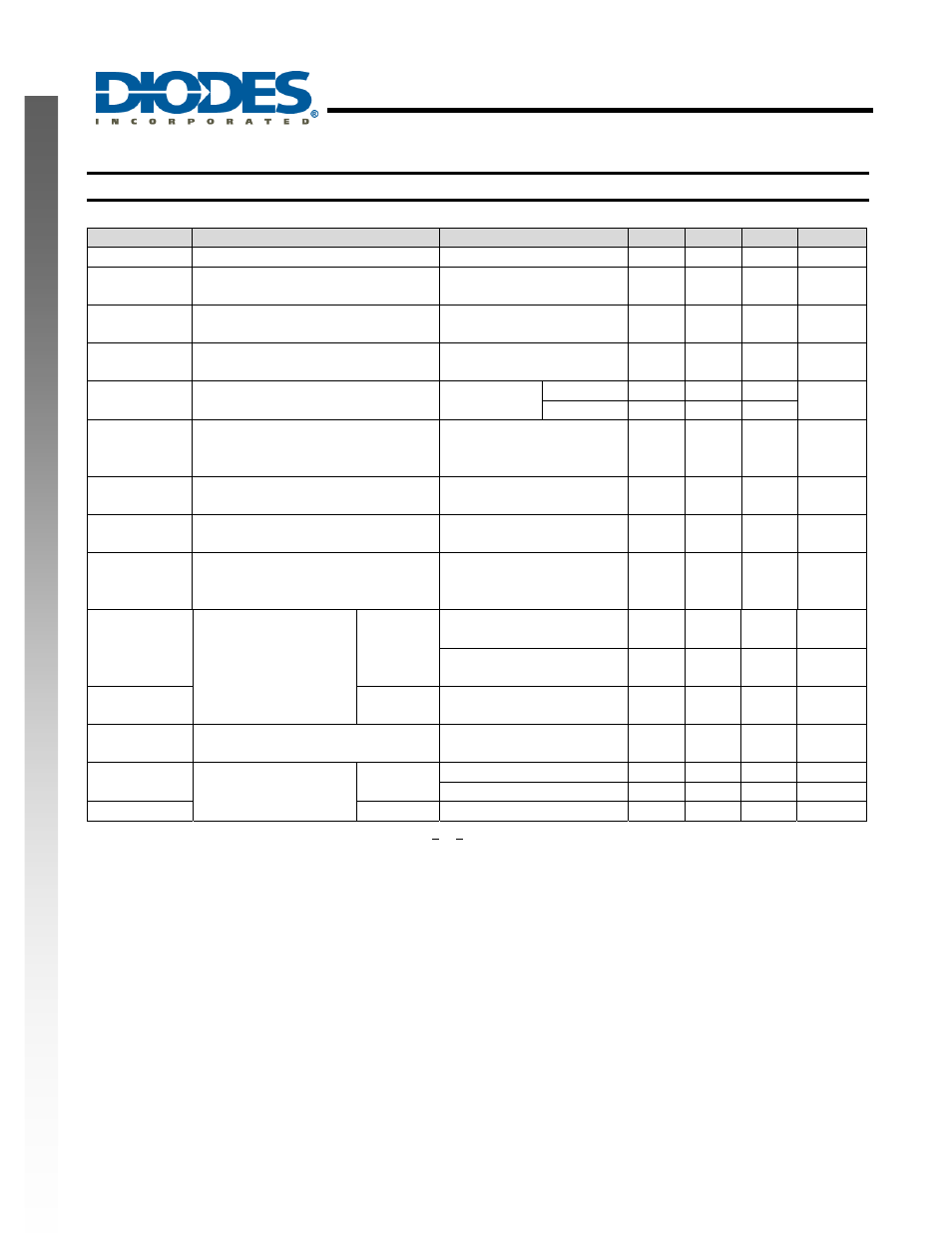
Electrical Characteristics
(T
A
= 25
o
C, V
+
= +5.0V, unless otherwise stated) (Note 5)
Symbol
Parameter
Conditions
Min
Typ.
Max
Unit
V
IO
Input Offset Voltage
T
A
= 25
o
C,
(Note 6)
- 2 7 mV
I
B
Input Bias Current
I
IN(+)
or I
IN(
−)
, T
A
= 25°C, V
CM
=
0V,
(Note 7)
- 45
250 nA
I
IO
Input Offset Current
I
IN(+)
- I
IN(
−)
,V
CM
= 0V,
T
A
= 25°C
- 5 50 nA
V
ICM
Input Common-Mode Voltage Range
V
+
= 30V,
(Note 8)
T
A
= 25°C
0 -
V
+
-1.5
V
I
S
Supply Current
Over Full Temperature Range
R
L
=
∞ on All
Op Amps
V
+
= 30V
-
1
2
mA
V
+
= 5V
-
0.5
1.2
A
V
Large Signal Voltage Gain
V
+
= 15V, T
A
= 25°C,
R
L
> 2k
Ω,
(For V
O
= 1V to 11V)
25 100 - V/mV
CMRR
Common-Mode Rejection Ratio
T
A
= 25°C, V
CM
= 0V to
V
+
-1.5V
65 85 - dB
PSRR
Power Supply Rejection Ratio
V
+
= 5V to 30V,
T
A
= 25°C
65 100 -
dB
Amplifier-to-Amplifier
Coupling
f = 1KHz to 20 KHz,
T
A
= 25°C
(Input Referred)
(Note 9)
- -120 - dB
I
SINK
Output Current
Sink
V
IN(-)
= 1V, V
IN(+)
= 0V, V
+
=
15V, V
O
= 2V, T
A
= 25°C
10 20 - mA
V
IN(-)
= 1V, V
IN(+)
= 0V, V
+
=
15V, V
O
= 200mV, T
A
= 25°C
20 70 -
μA
I
SOURCE
Source
V
IN(+)
= 1V, V
IN(-)
= 0V, V
+
=
15V, V
O
= 2V, T
A
= 25°C
20 40 - mA
I
SC
Short Circuit to Ground
T
A
= 25°C,
(Note 10)
V
+
= 15V
- 40 60 mA
V
OH
Output Voltage Swing
(V
+
=30V)
R
L
= 2k
Ω, T
A
= 25
o
C
26 - - V
R
L
= 10k
Ω, T
A
= 25
o
C
27 28 -
V
V
OL
(V
+
=5V) R
L
= 10k
Ω, T
A
= 25
o
C
- 5 20 mV
Notes: 5. The LM358 temperature specifications are limited to 0°C < T
A
< +70°C.
6. V
O
≅
1.4V, R
S
= 0
Ω with V
+
from 5V to 30V; and over the full input common-mode range (0V to V
+
-1.5V) at 25°C.
7. The direction of the input current is out of the IC due to the PNP input stage. This current is essentially constant, independent of the state of the
output so no loading change exists on the input lines.
8. The input common-mode voltage of either input signal voltage should not be allowed to go negative by more than 0.3V (at25°C). The upper end of
the common-mode voltage range is V
+
-1.5V (at 25°C), but either or both inputs can go to +32V without damage, independent of the magnitude of V
+
.
9. Due to proximity of external components, insure that coupling is not originating via stray capacitance between these external parts. This typically can
be detected as this type of capacitance increases at higher frequencies.
10.Short circuits from the output to V
+
can cause excessive heating and eventual destruction. When considering short circuits to ground, the output
maximum current is approximately 40mA independent of the magnitude of V
+
. At values of supply voltage in excess of +15V, continuous short-
circuits can exceed the power dissipation ratings and cause eventual destruction. Destructive dissipation can result from simultaneous shorts on all
amplifiers.