Schematic diagram, Pin descriptions – Diodes LM2901/ LM2901A/ LM2903/ LM2903A User Manual
Page 2
LM2901/ LM2901A/ LM2903/ LM2903A
Document number: DS36779 Rev. 1 - 2
2 of 15
March 2014
© Diodes Incorporated
LM2901/ LM2901A/ LM2903/ LM2903A
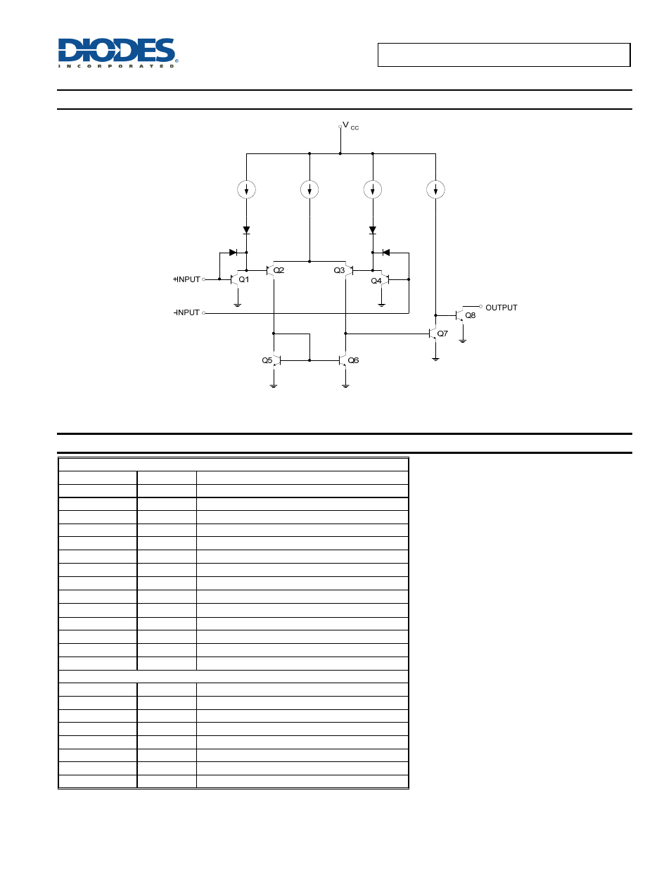
Schematic Diagram
Functional Block Diagram of LM2901/2901A/2903/2903A
(Each Comparator)
Pin Descriptions
LM2901, LM2901A
Pin Name
Pin #
Function
1OUT 1
Channel
1
Output
2OUT 2
Channel
2
Output
V
CC
3
Chip Supply Voltage
2IN-
4
Channel 2 Inverting Input
2IN+
5
Channel 2 Non-inverting Input
1IN-
6
Channel 1 Inverting Input
1IN+
7
Channel 1 Non-inverting Input
3IN-
8
Channel 3 Inverting Input
3IN+
9
Channel 3 Non-inverting Input
4IN-
10
Channel 4 Inverting Input
4IN+
11
Channel 4 Non-inverting Input
GND 12
Ground
4OUT 13
Channel
4
Output
3OUT 14
Channel
3
Output
LM2903, LM2903A
1OUT
1
Channel 1 Output
1IN-
2
Channel 1 Inverting Input
1IN+
3
Channel 1 Non-inverting Input
GND 4
Ground
2IN+
5
Channel 2 Non-inverting Input
2IN-
6
Channel 2 Inverting Input
2OUT 7
Channel
2
Output
V
CC
8
Chip Supply Voltage