Electrical characteristics, Ac electrical characteristics – Diodes LM2902/ LM2902A/ LM2904/ LM2904A User Manual
Page 4
LM2902/ LM2902A/ LM2904/ LM2904A
Document number: DS36780 Rev. 1 - 2
4 of 13
March 2014
© Diodes Incorporated
LM2902/ LM2902A/ LM2904/ LM2904A
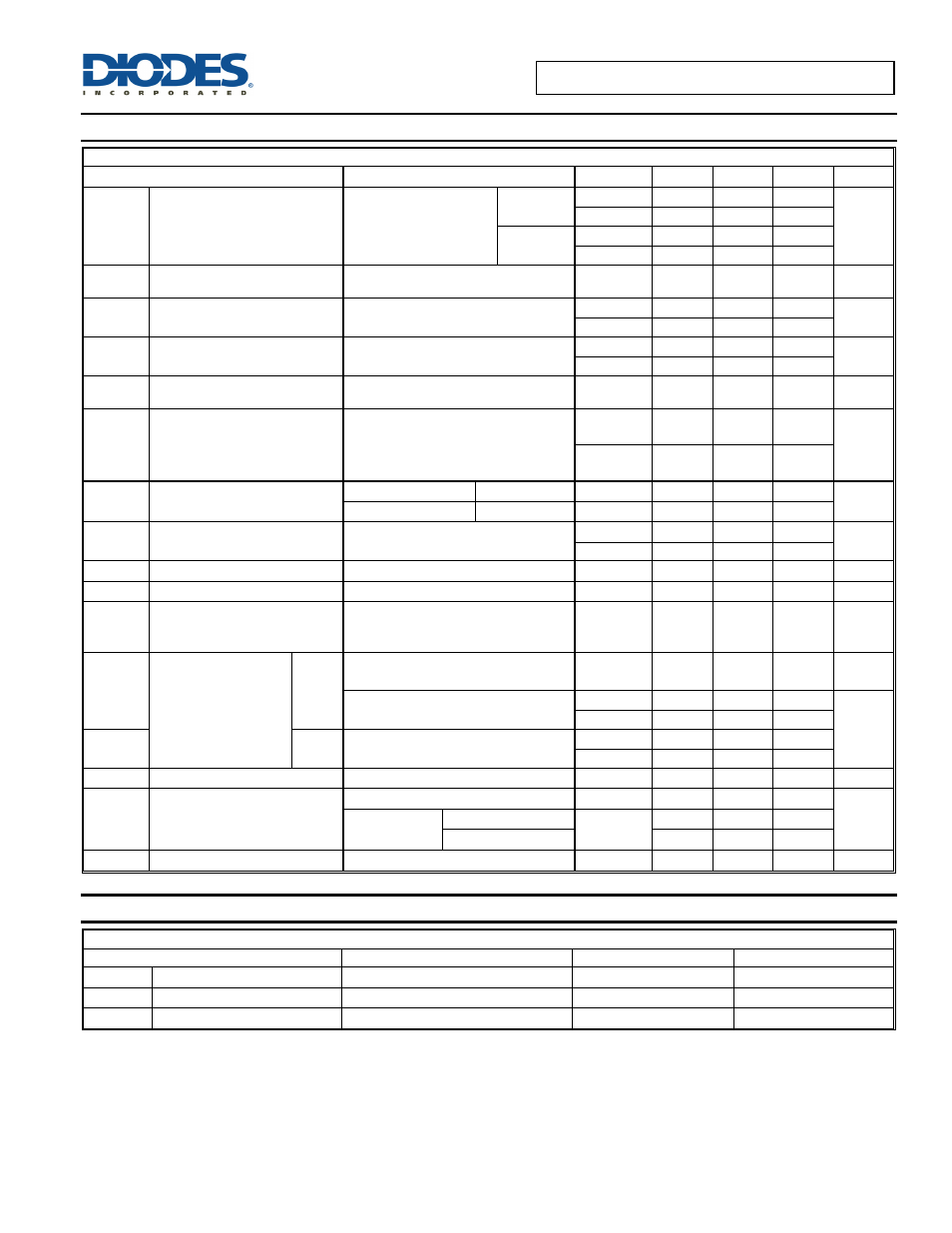
Electrical Characteristics
(Notes 12 & 13) (@ V
CC
= +5.0V, T
A
= +25°C, unless otherwise specified.)
LM2902, LM2902A
Parameter Conditions
T
A
Min Typ Max Unit
V
IO
Input Offset Voltage
V
IC
= V
CMR
min,
V
O
= 1.4V,
V
CC
= 5V to MAX
Rs = 0Ω
Non-A
Device
T
A
= +25°C
— 2 7
mV
Full range
—
—
10
A-Suffix
Device
T
A
= +25°C
— 1 2
Full range
—
—
4
∆V
IO
/∆T
Input Offset Voltage Temperature
Drift
Rs = 0Ω Full
range
—
7
—
µV/
℃
I
B
Input Bias Current
I
IN+
or I
IN−
with OUT in linear range,
V
CMR
= 0V (Note 9)
T
A
= +25°C
—
-20 -200
nA
Full range
—
—
-500
I
IO
Input Offset Current
I
IN+
- I
IN−
, V
CM
= 0V
T
A
= +25°C
—
2 50
nA
Full range
—
—
150
∆I
IO
/∆T
Input Offset Current Temperature
Drift
— Full
range
—
10
—
pA/
℃
V
CMR
Input Common-Mode Voltage
Range
V
CC
= 30V (Note 10)
T
A
= +25°C
0 to
V
CC
-1.5
— —
V
Full range
0 to
V
CC
-2.0
— —
I
CC
Supply Current
(Four Amplifiers)
V
O
= 0.5V
CC
, No Load V
CC
= 30V
Full range
—
1.0 3.0
mA
V
O
= 0.5V
CC
,
No Load V
CC
= 5V
Full range
—
0.7 1.2
A
V
Voltage Gain
V
CC
= 15V, V
OUT
= 1V to 11V,
R
L
≥ 2kΩ
T
A
= +25°C
25 100 —
V/mV
Full range
15
—
—
CMRR Common Mode Rejection Ratio
DC, V
CMR
= 0V to V
CC
-1.5V T
A
= +25°C
60 70 —
dB
PSRR
Power Supply Rejection Ratio
V
CC
= 5V to 30V
T
A
= +25°C
70 100 —
dB
Amplifier to Amplifier Coupling
f = 1kHz to 20kHz
(Input Referred)
(Note 11)
T
A
= +25°C
— -120 — dB
I
SINK
Output Current
Sink
V
IN
-
= 1V, V
IN
+
= 0V, V
CC
= 15V,
V
O
= 200mV
T
A
= +25°C
12 50 — µA
V
IN
-
= 1V, V
IN
+
= 0V, V
CC
= 15V,
V
O
= 15V
T
A
= +25°C
10 20 —
mA
Full range
5
—
—
I
SOURCE
Source
V
IN
+
= 1V, V
IN
-
= 0V, V
CC
= 15V,
V
O
= 0V
T
A
= +25°C
-20 -40 -60
Full range
-10
—
—
I
SC
Short-Circuit to Ground
V
CC
= 5V, GND = -5V, V
O
= 0V
T
A
= +25°C
—
±40 ±60 mA
V
OH
High-Level Output Voltage Swing
R
L
= 10KΩ
T
A
= +25°C
—
V
CC
-1.5
—
V
V
CC
= 30V
R
L
= 2KΩ,
Full range
26
— —
R
L
≥ 10KΩ
27 28 —
V
OL
Low-Lever Output Voltage Swing R
L
≦ 10KΩ
Full range
—
5
20
mV
AC Electrical Characteristics
(Notes 12 & 13) (@ V
CC
= ±15.0V, T
A
= +25°C, unless otherwise specified.)
LM2902, LM2902A
Parameter Conditions
Typ
Unit
SR
Slew Rate at Unity Gain
R
L
= 1MΩ, C
L
= 30pF, V
I
= ±10V
0.3
V/µs
B1 Unity
Gain
Bandwidth
R
L
= 1MΩ, C
L
= 20pF
0.7
MHz
Vn
Equivalent Input Noise Voltage
R
S
= 100Ω, V
I
= 0V, f = 1KHz
40
nV/√Hz
Notes:
9. The direction of the input current is out of the IC due to the PNP input stage. This current is essentially constant, independent of the state of the
output so no loading change exists on the input lines.
10. The input common-mode voltage of either input signal voltage should not be allowed to go negative by more than 0.3V (@ +25°C). The upper end of the
common-mode voltage range is V
CC
-1.5V (@ 25°C), but either or both inputs can go to +36V without damage, independent of the magnitude of V
CC
.
11. Due to proximity of external components, insure that coupling is not originating via stray capacitance between these external parts. This typically can
be detected as this type of capacitance increases at higher frequencies.
12. Typical values are all at T
A
=25°C conditions and represent the most likely parametric norm as determined at the time of characterization. Actual
typical values may vary over time and will also depend on the application and configuration. The typical values are not tested and are not guaranteed
on shipped production material.
13. All limits are guaranteed by testing or statistical analysis. Limits over the full temperature are guaranteed by design, but not tested in production.