Maximum ratings, total device, Maximum ratings, npn transistor, Maximum ratings, zener element – Diodes DVR5V0W User Manual
Page 2: Electrical characteristics, npn transistor, Electrical characteristics, zener element, Dvr5v0w
DVR5V0W
Document number: DS30578 Rev. 6 - 2
2 of 5
July 2011
© Diodes Incorporated
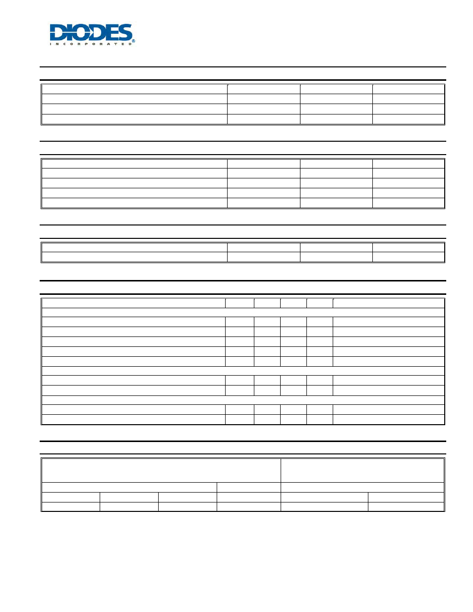
Maximum Ratings, Total Device
@T
A
= 25°C unless otherwise specified
Characteristic
Symbol
Value
Unit
Power Dissipation (Note 4)
P
d
200
mW
Thermal Resistance, Junction to Ambient (Note 4)
R
θJA
625
°C/W
Operating and Storage Temperature Range
T
j
, T
STG
-55 to +150
°C
Maximum Ratings, NPN Transistor
@T
A
= 25°C unless otherwise specified
Characteristic
Symbol
Value
Unit
Collector-Base Voltage
V
CBO
45
V
Collector-Emitter Voltage
V
CEO
18
V
Emitter-Base Voltage
V
EBO
5
V
Collector Current - Continuous (Note 4)
I
C
1
A
Maximum Ratings, Zener Element
@T
A
= 25°C unless otherwise specified
Characteristic
Symbol
Value
Unit
Forward Voltage @ I
F
= 10mA
V
F
0.9
V
Electrical Characteristics, NPN Transistor
@T
A
= 25°C unless otherwise specified
Characteristic
Symbol
Min
Max
Unit
Test Condition
OFF CHARACTERISTICS (Note 5)
Collector-Base Breakdown Voltage
V
(BR)CBO
45
⎯
V
I
C
= 100
μA, I
E
= 0
Collector-Emitter Breakdown Voltage
V
(BR)CEO
18
⎯
V
I
C
= 1mA, I
B
= 0
Emitter-Base Breakdown Voltage
V
(BR)EBO
5
⎯
V
I
E
= 100
μA, I
C
= 0
Collector Cutoff Current
I
CBO
⎯
1
μA
V
CB
= 40V, I
E
= 0
Emitter Cutoff Current
I
EBO
⎯
1
μA
V
EB
= 4V, I
C
= 0
ON CHARACTERISTICS (Note 5)
DC Current Gain
h
FE
150
800
⎯
I
C
= 100mA, V
CE
= 1V
Collector-Emitter Saturation Voltage
V
CE(SAT)
⎯
0.5
V
I
C
= 300mA, I
B
= 30mA
SMALL SIGNAL CHARACTERISTICS
Output Capacitance
C
obo
⎯
8
pF
V
CB
= 10V, f = 1.0MHz, I
E
= 0
Current Gain-Bandwidth Product
f
T
100
⎯
MHz
V
CB
= 10V, I
E
= 50mA, f = 100MHz
Electrical Characteristics, Zener Element
@T
A
= 25°C unless otherwise specified
Zener Voltage Range
(Note 6)
Maximum Reverse
Leakage Current
(Note 5)
V
Z
@ I
ZT
I
ZT
I
R
@ V
R
Nom (V)
Min (V)
Max (V)
mA
μA
V
5.1
4.85
5.36
0.05
5
3
Notes:
4. Part mounted on FR-4 board with recommended pad layout, which can be found on our website at
5. Short duration pulse test used to minimize self-heating effect.
6. Nominal Zener voltage is measured with the device junction in thermal equilibrium at T
T
= 30°C ±1°C.