Maximum ratings, Thermal characteristics, Electrical characteristics – Diodes DESD1P0RFW User Manual
Page 2
DESD1P0RFW
Document number: DS35278 Rev. 5 - 2
2 of 4
September 2011
© Diodes Incorporated
DESD1P0RFW
ADVAN
CE I
N
F
O
RM
ATI
O
N
Maximum Ratings
@T
A
= 25°C unless otherwise specified
Characteristic Symbol
Value
Unit
Conditions
Peak Pulse Current
I
PP
15 A
8/20
μs (Notes 4 & 5)
ESD Protection – Contact Discharge
V
ESD_Contact
±30
kV
Standard IEC 61000-4-2(Note 5)
ESD Protection – Air Discharge
V
ESD_Air
±30
kV
Standard IEC 61000-4-2(Note 5)
Thermal Characteristics
Characteristic Symbol
Value
Unit
Power Dissipation (Note 6)
P
D
200 mW
Thermal Resistance Junction to Ambient Air (Note 6)
R
θJA
625
°C/W
Operating and Storage Temperature Range
T
J
, T
STG
-65 to +150
°C
Electrical Characteristics
@T
A
= 25°C unless otherwise specified
Characteristic (Note 4)
Symbol
Min
Typ
Max
Unit
Test Conditions
Reverse Working Voltage
V
RWM
- - 70 V
-
Reverse Current
I
RM
- - 100 nA
V
RM
= 70V
Forward Clamping Voltage (Note 5)
V
FC
- 2 6
V
I
PP
= 3A; per IEC 61000-4-5 (Note 7)
- 4 8
I
PP
= 10A; per IEC 61000-4-5 (Note 7)
Capacitance
C
T
- 1 1.5 pF
V
R
= 0V, f = 1MHz (Note 8)
Notes:
4. Diodes Short duration pulse test used to minimize self-heating effect.
5. Anti-parallel or rail-to-rail connection
6. Device mounted on FR-4 PCB with minimum recommended pad layout.
7. Clamping voltage value is based on an 8x20
μs peak pulse current (I
pp
) waveform.
8. Total capacitance line to ground (2 diodes in parallel)
0
50
100
150
200
250
P
,
P
O
WE
R
DI
SSI
P
A
T
IO
N (
m
W
)
D
T , AMBIENT TEMPERATURE ( C)
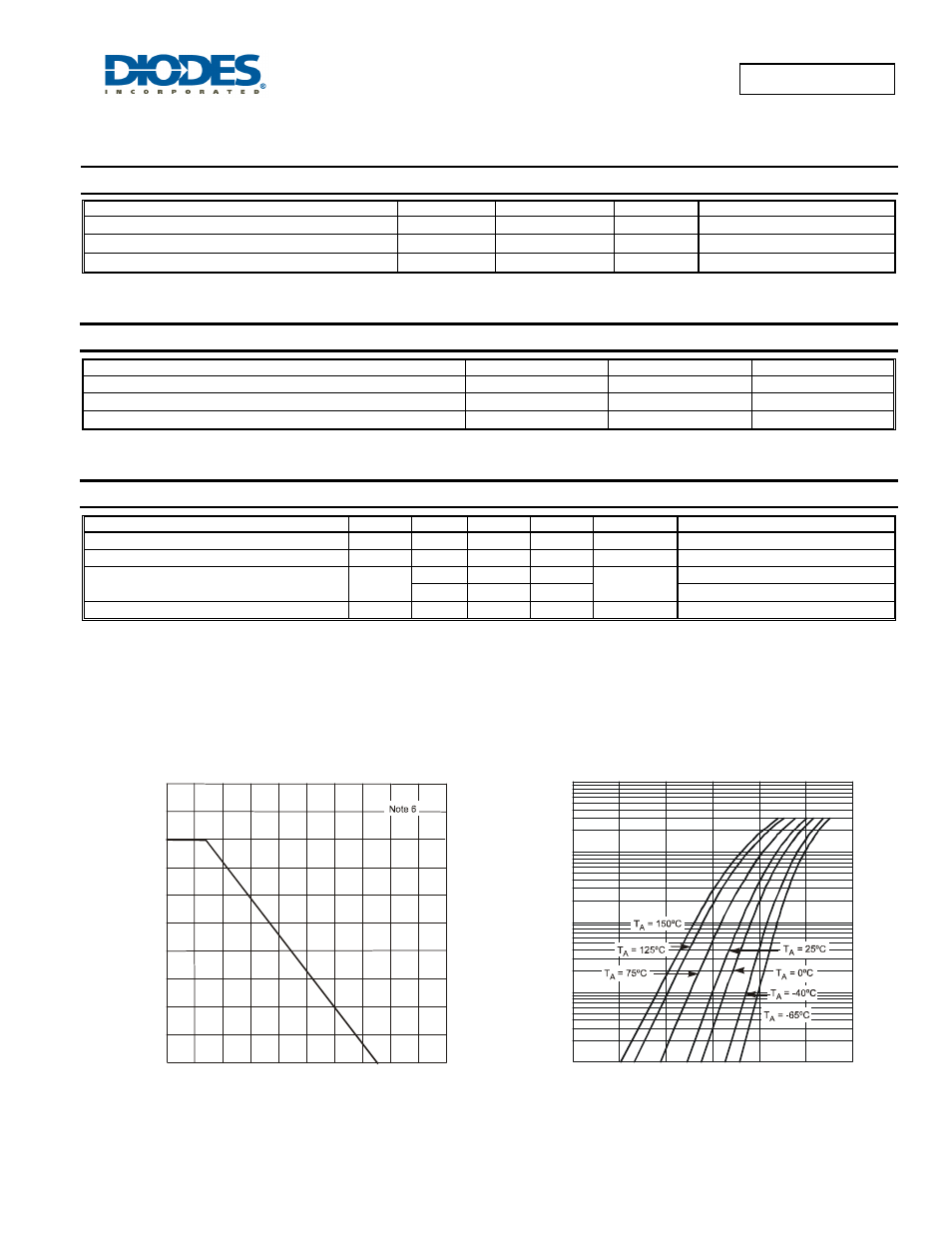
Fig. 1 Power Derating Curve, Total Package
A
°
0
120
160
200
40
80
0.1
1
10
100
1,000
0
0.2
0.4
0.6
0.8
1.0
1.2
V , INSTANTANEOUS FORWARD VOLTAGE (V)
Fig. 2 Typical Forward Characteristics, Per Element
F
I,
I
N
S
T
AN
T
AN
E
O
U
S F
O
R
WA
R
D
C
U
R
R
EN
T
(mA
)
F