Dzqa6v8axv5, Maximum ratings, Thermal characteristics – Diodes DZQA6V8AXV5 User Manual
Page 2: Electrical characteristics
DZQA6V8AXV5
Document number: DS31271 Rev. 6 - 2
2 of 4
February 2011
© Diodes Incorporated
DZQA6V8AXV5
Maximum Ratings
@T
A
= 25°C unless otherwise specified
Characteristic Symbol
Value
Unit
Forward Voltage @ I
F
= 10mA
V
F
0.9 V
Thermal Characteristics
Characteristic Symbol
Value
Unit
Power Dissipation (Notes 4 & 5)
P
D
380 mW
Peak Power Dissipation, 8x20
μS Waveform (Note 6)
P
pk
20 W
Thermal Resistance, Junction-to-Ambient (Note 4)
R
θJA
327 °C/W
Operating and Storage Temperature Range
T
J,
T
STG
-55 to +150
°C
Electrical Characteristics
@T
A
= 25°C unless otherwise specified
Type
Number
Marking
Code
Breakdown Voltage
(Note 7)
Leakage Current
(Note 7)
Clamping
Voltage
(Note 6)
Capacitance
@0V Bias(pF)
(Note 8)
Capacitance
@3V Bias(pF)
(Note 8)
V
BR
@ I
T
= 1mA
I
RM
@ V
RM
V
C
Max @ I
PP
C
T
C
T
Min (V)
Nom (V) Max (V)
Max(
μA)
(V)
V
C
(V) I
PP
(A)
Typ Max Typ Max
DZQA6V8AXV5
T62 6.47 6.8 7.14 1
4.3 13
1.6
12.5 15 7.6 9.5
Notes:
4. Device mounted on FR-4 PCB, 1 inch x 0.85 inch x 0.062 inch; pad layout as shown on Diodes Inc. Suggested Pad Layout Document AP02001,
which can be found on our website at
5. Only 1 diode under power. For all 4 diodes under power, P
D
will be 25% of the listed value.
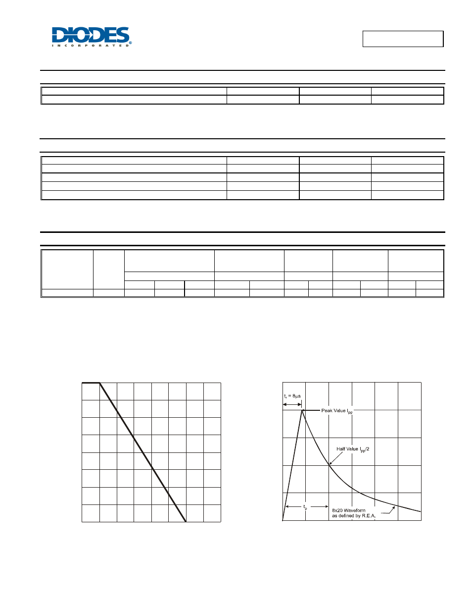
6. Non-repetitive current pulse per Figure 3 and derate above T
A
= 25°C per Figure 1.
7. Short duration pulse test used to minimize self-heating effect.
8. Per element, f = 1MHz, T
A
= 25
°C
0
25
50
75
100
125
150
175
200
100
75
50
25
0
T , AMBIENT TEMPERATURE (°C)
Fig. 1 Pulse Derating Curve
A
P
EA
K
P
U
L
SE DE
R
A
T
IN
G
IN %
O
F
PEA
K POW
E
R OR
CURR
ENT
0
t, TIME ( s)
Fig. 2 Pulse Waveform
μ
20
40
60
100
50
0
I
, PE
AK P
U
L
S
E
CURRENT
(
%
I
)
Pp
p
P