Diodes DESD5V2S2UT User Manual
Desd5v2s2ut new prod uc t, Features, Mechanical data
DESD5V2S2UT
Document number: DS31791 Rev. 3 - 2
1 of 4
September 2009
© Diodes Incorporated
DESD5V2S2UT
NEW PROD
UC
T
UNIDIRECTIONAL SURFACE MOUNT TVS
Features
•
260 Watts Peak Pulse Power (tp = 8x20
μs)
•
61000-4-2 (ESD): Air – 30kV, Contact – 30kV
•
MIL-STD 883(ESD), HBM – 10kV
•
Low Reverse Leakage Current, I
R
< 1
μA
• Unidirectional
Configuration
•
Lead Free/RoHS Compliant (Note 3)
•
“Green” Device (Note 4)
•
Qualified to AEC-Q101 Standards for High Reliability
Mechanical Data
• Case:
SOT-23
•
Case Material: Molded Plastic, “Green” Molding Compound,
Note 3. UL Flammability Classification Rating 94V-0
•
Moisture Sensitivity: Level 1 per J-STD-020
•
Terminals: Matte Tin Finish annealed over Alloy 42 leadframe
(Lead Free Plating). Solderable per MIL-STD-202, Method 208
•
Ordering Information: See Page 2
•
Marking Information: See Page 2
•
Weight: 0.0089 grams (approximate)
Thermal Characteristics – Total Device
Characteristic Symbol
Value
Unit
Peak Pulse Power (tp = 8x20
μs) (Note 6) T
A
= 25°C
P
pk
260 W
Thermal Resistance, Junction to Ambient (Note 6) T
A
= 25°C
R
θJA
417
°C/W
Operating and Storage Temperature Range
T
J
, T
STG
-65 to +150
°C
Electrical Characteristics
@T
A
= 25°C unless otherwise specified
Reverse
Standoff
Voltage
Breakdown
Voltage
V
BR
@ I
T
Test
Current
Max. Reverse
Leakage @ V
RWM
(Note 5)
Max. Clamping
Voltage @ I
pp
= 1A
(Note 2)
Max. Clamping
Voltage V
C
@
I
PP
(Note 2)
Typical Total
Capacitance C
T
(Note 1)
Maximum Total
Capacitance C
T
(Note 1)
V
RWM
(V)
Min (V) Max (V)
I
T
(mA)
I
R
(
μA) V
C
(V)
V
C
(V)
I
PP
(A) (pF)
(pF)
5.2 6.4
7.2 5.0
1
9
20
15
165
200
Notes: 1.
V
R
= 0V, f = 1MHz.
2. Clamping voltage value is based on an 8x20
μs peak pulse current (I
pp
) waveform.
3. No purposefully added lead.
4. Diodes Inc.’s “Green” policy can be found on our websit5. Short duration pulse test used to minimize self-heating effect.
6. Device mounted on FR-4 PC board with suggested pad layout, which can be found on our website at7. Measured across either pin 1 and pin 3 or pin 2 and pin 3.
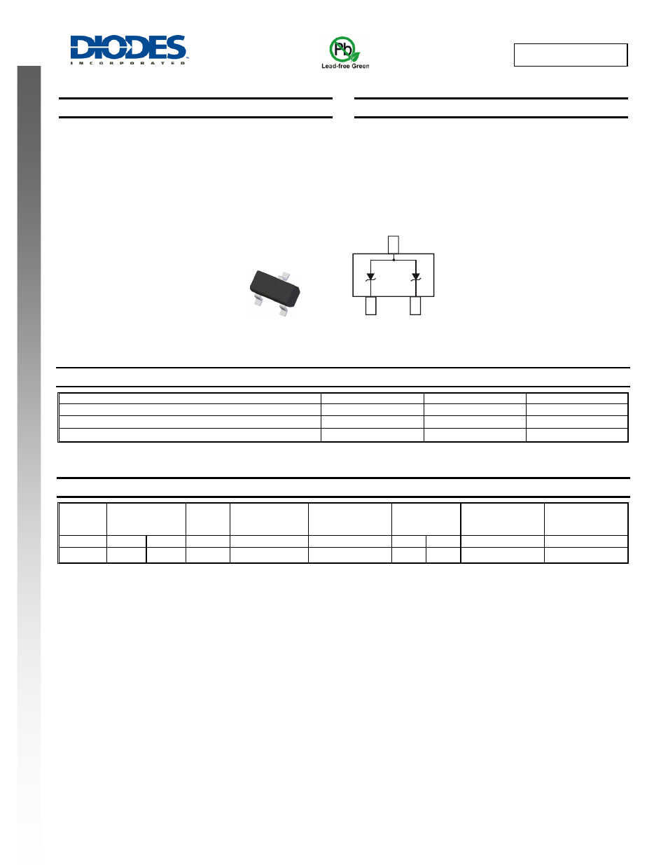
Top View
Device Schematic
2
1
3