Maximum ratings, Thermal characteristics, Electrical characteristics – Diodes DMG4710SSS User Manual
Page 2: Dmg4710sss
DMG4710SSS
Document number: DS32055 Rev. 6 - 2
2 of 6
November 2010
© Diodes Incorporated
DMG4710SSS
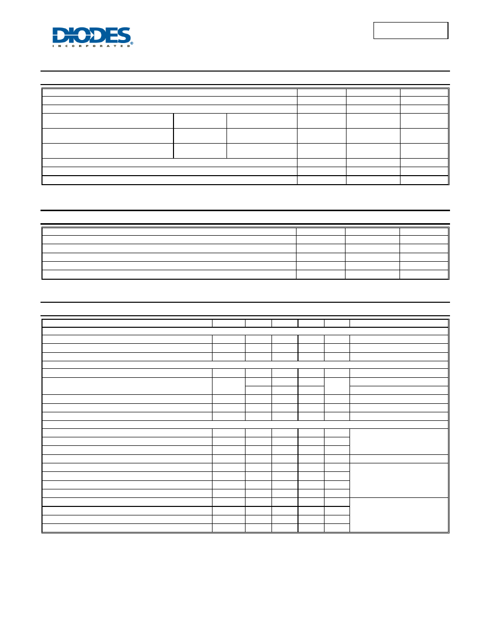
Maximum Ratings
@T
A
= 25°C unless otherwise specified
Characteristic
Symbol
Value
Unit
Drain-Source Voltage
V
DSS
30 V
Gate-Source Voltage
V
GSS
±12 V
Continuous Drain Current (Note 4) V
GS
= 10V
Steady
State
T
A
= 25°C
T
A
= 85°C
I
D
8.8
6.3
A
Continuous Drain Current (Note 5) V
GS
= 10V
t
≤ 10 sec
T
A
= 25°C
T
A
= 85°C
I
D
11.7
8.5
A
Continuous Drain Current (Note 5) V
GS
= 4.5V
t
≤ 10 sec
T
A
= 25°C
T
A
= 85°C
I
D
10.8
7.8
A
Pulsed Drain Current (Note 6)
I
DM
90 A
Avalanche Current (Notes 6 & 7)
I
AR
13 A
Repetitive Avalanche Energy (Notes 6 & 7) L = 0.3mH
E
AR
25.4 mJ
Thermal Characteristics
Characteristic Symbol
Value
Unit
Power Dissipation (Note 4)
P
D
1.54 W
Thermal Resistance, Junction to Ambient @T
A
= 25°C (Note 4)
R
θJA
81 °C/W
Power Dissipation (Note 5)
P
D
2.8 W
Thermal Resistance, Junction to Ambient @T
A
= 25°C (Note 5)
R
θJA
45 °C/W
Operating and Storage Temperature Range
T
J
,
T
STG
-55 to +150
°C
Electrical Characteristics
@
T
A
= 25°C unless otherwise stated
Characteristic
Symbol
Min
Typ
Max
Unit
Test Condition
OFF CHARACTERISTICS (Note 8)
Drain-Source Breakdown Voltage
BV
DSS
30 - - V
V
GS
= 0V, I
D
= 1mA
Zero Gate Voltage Drain Current
I
DSS
- -
0.1
mA
V
DS
= 30V, V
GS
= 0V
Gate-Source Leakage
I
GSS
- -
±100
nA
V
GS
= ±12V, V
DS
= 0V
ON CHARACTERISTICS (Note 8)
Gate Threshold Voltage
V
GS(th)
1.0 - 2.3 V
V
DS
= V
GS
, I
D
= 250
μA
Static Drain-Source On-Resistance
R
DS (ON)
- 9.5
12.5
mΩ
V
GS
= 10V, I
D
= 11.7A
- 11.5
14.8
V
GS
= 4.5V, I
D
= 10.8A
Forward Transfer Admittance
|Y
fs
|
- 22 - S
V
DS
= 5V, I
D
= 11.7A
Diode Forward Voltage
V
SD
- 0.38
0.6 V
V
GS
= 0V, I
S
= 1A
Maximum Body-Diode + Schottky Continuous Current
I
S
- - 5 A
-
DYNAMIC CHARACTERISTICS (Note 9)
Input Capacitance
C
iss
- 1849 - pF
V
DS
=15V, V
GS
= 0V,
f = 1.0MHz
Output Capacitance
C
oss
- 158 - pF
Reverse Transfer Capacitance
C
rss
- 123 - pF
Gate Resistance
R
g
0.54 2.68 4.82 Ω
V
DS
=0V, V
GS
= 0V, f = 1MHz
Total Gate Charge V
GS
= 4.5V
Q
g
- 18.5 - nC
V
DS
= 15V, V
GS
= 10V,
I
D
= 11.7A
Total Gate Charge V
GS
= 10V
Q
g
- 43 - nC
Gate-Source Charge
Q
gs
- 4.7 - nC
Gate-Drain Charge
Q
gd
- 4.0 - nC
Turn-On Delay Time
t
D(on)
- 6.62 - ns
V
GS
= 10V, V
DS
= 10V,
R
G
= 3
Ω, R
L
= 1.2
Ω
Turn-On Rise Time
t
r
- 8.73 - ns
Turn-Off Delay Time
t
D(off)
- 36.41 - ns
Turn-Off Fall Time
t
f
- 4.69 - ns
Notes:
4. Device mounted on FR-4 PCB with minimum recommended pad layout. The value in any given application depends on the user’s specific board design.
5. Device mounted on 1” x 1” FR-4 PCB with high coverage 1 oz. Copper, single sided , device is measured at t
≤ 10 sec.
6. Repetitive rating, pulse width limited by junction temperature.
7. I
AR
and E
AR
rating are based on low frequency and duty cycles to keep T
J
= 25°C
8. Short duration pulse test used to minimize self-heating effect.
9. Guaranteed by design. Not subject to production testing.