Maximum ratings – total device, Maximum ratings – p-channel mosfet – q1, Maximum ratings – sbr – d1 – Diodes DMS2220LFDB User Manual
Page 2: Electrical characteristics – p-channel mosfet – q1, Electrical characteristics – sbr – d1, Dms2220lfdb
SBR is a registered trademark of Diodes Incorporated.
DMS2220LFDB
Document number: DS31546 Rev. 9 - 2
2 of 7
January 2013
© Diodes Incorporated
DMS2220LFDB
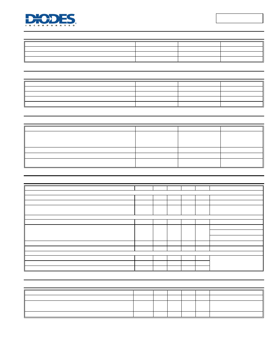
Maximum Ratings – TOTAL DEVICE
(@T
A
= +25°C, unless otherwise specified.)
Characteristic Symbol
Value
Unit
Power Dissipation (Note 5)
P
D
1.4 W
Thermal Resistance, Junction to Ambient
R
θJA
89 °C/W
Operating and Storage Temperature Range
T
J
, T
STG
-55 to +150
°C
Maximum Ratings – P-CHANNEL MOSFET – Q1
(@T
A
= +25°C, unless otherwise specified.)
Characteristic Symbol
Value
Units
Drain-Source Voltage
V
DSS
-20 V
Gate-Source Voltage
V
GSS
±12 V
Drain Current (Note 5)
I
D
-3.5 A
Pulsed Drain Current (Note 6)
I
DM
-12 A
Maximum Ratings – SBR – D1
(@T
A
= +25°C, unless otherwise specified.)
Characteristic Symbol
Value
Unit
Peak Repetitive Reverse Voltage
Working Peak Reverse Voltage
DC Blocking Voltage
V
RRM
V
RWM
V
R
20 V
RMS Reverse Voltage
V
R(RMS)
14 V
Average Rectified Output Current
I
O
1 A
Non-Repetitive Peak Forward Surge Current
8.3ms single half sine-wave superimposed on rated load
I
FSM
3 A
Electrical Characteristics – P-CHANNEL MOSFET – Q1
(@T
A
= +25°C, unless otherwise specified.)
Characteristic Symbol
Min
Typ
Max
Unit
Test
Condition
OFF CHARACTERISTICS (Note 7)
Drain-Source Breakdown Voltage
BV
DSS
-20 — — V
V
GS
= 0V, I
D
= -250µA
Zero Gate Voltage Drain Current
I
DSS
— — -1 µA
V
DS
= -20V, V
GS
= 0V
Gate-Source Leakage
I
GSS
—
—
—
—
±100
±800
nA
V
GS
= ±8V, V
DS
= 0V
V
GS
= ±12V, V
DS
= 0V
ON CHARACTERISTICS (Note 7)
Gate Threshold Voltage
V
GS(th)
-0.45 — -1.3 V V
DS
= V
GS
, I
D
= -250µA
Static Drain-Source On-Resistance
R
DS(ON)
—
—
—
60
74
86
95
120
—
mΩ
V
GS
= -4.5V, I
D
= -2.8A
V
GS
= -2.5V, I
D
= -2.0A
V
GS
= -1.8V, I
D
= -1.0A
Forward Transfer Admittance
|Y
fs
|
— 8 — S
V
DS
= -5V, I
D
= -2.8A
Diode Forward Voltage (Note 7)
V
SD
— 0.7 -1.2 V
V
GS
= 0V, I
S
= -1.6A
DYNAMIC CHARACTERISTICS
Input Capacitance
C
iss
— 632 — pF
V
DS
= -10V, V
GS
= 0V
f = 1.0MHz
Output Capacitance
C
oss
— 65 — pF
Reverse Transfer Capacitance
C
rss
— 54 — pF
Electrical Characteristics – SBR – D1
(@T
A
= +25°C, unless otherwise specified.)
Characteristic Symbol
Min
Typ
Max
Unit
Test
Condition
Reverse Breakdown Voltage (Note 7)
V
(BR)R
20 — — V
I
R
= 1mA
Forward Voltage
V
F
—
—
—
—
0.45
0.52
V
I
F
= 0.5A
I
F
= 1.0A
Reverse Current (Note 7)
I
R
— — 100 µA
V
R
= 20V
Notes:
5. Device mounted on FR-4 PCB, on minimum recommended, 2oz Copper pad layout.
6. Repetitive rating, pulse width limited by junction temperature.
7. Short duration pulse test used to minimize self-heating effect.