Diodes DMC4029SSD User Manual
Product summary, Description, Applications
DMC4029SSD
Document number: DS36350 Rev. 3 - 2
1 of 8
March 2014
© Diodes Incorporated
DMC4029SSD
ADVAN
CE I
N
F
O
RM
ATI
O
N
NEW PROD
UC
T
COMPLEMENTARY PAIR ENHANCEMENT MODE MOSFET
Product Summary
Device
V
(BR)DSS
R
DS(on) max
I
D
T
A
= +25°C
Q2 40V
24m
Ω @ V
GS
= 10V
9.0A
32m
Ω @ V
GS
= 4.5V
7.8A
Q1 -40V
45m
Ω @ V
GS
= -10V
-6.5A
55m
Ω @ V
GS
= -4.5V
-5.9A
Description
This new generation MOSFET has been designed to minimize the on-
state resistance (R
DS(on)
) and yet maintain superior switching
performance, making it ideal for high efficiency power management
applications.
Applications
• DC-DC
Converters
•
Power Management Functions
• Backlighting
Features and Benefits
•
Low Input Capacitance
• Low
On-Resistance
•
Fast Switching Speed
•
Totally Lead-Free & Fully RoHS Compliant (Notes 1 & 2)
•
Halogen and Antimony Free. “Green” Device (Note 3)
•
Qualified to AEC-Q101 Standards for High Reliability
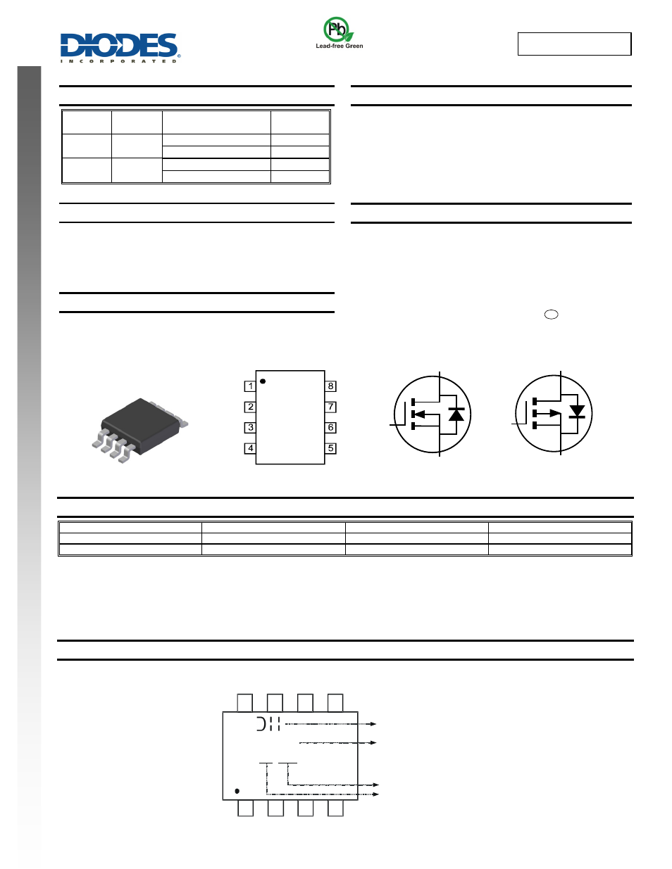
Mechanical Data
• Case:
SO-8
•
Case Material: Molded Plastic, “Green” Molding Compound.
UL Flammability Classification Rating 94V-0
•
Moisture Sensitivity: Level 1 per J-STD-020
•
Terminal Connections: See Diagram
•
Terminals: Finish – Tin Finish annealed over Copper leadframe.
Solderable per MIL-STD-202, Method 208
•
Weight: 0.074 grams (approximate)
Ordering Information
(Note 4 & 5)
Part Number
Compliance Case
Packaging
DMC4029SSD-13
Standard
SO-8
2,500/Tape & Reel
DMC4029SSDQ-13
Automotive
SO-8
2,500/Tape & Reel
Notes:
1. No purposely added lead. Fully EU Directive 2002/95/EC (RoHS) & 2011/65/EU (RoHS 2) compliant.
2. S more information about Diodes Incorporated’s definitions of Halogen- and Antimony-free, "Green"
and Lead-free.
3. Halogen- and Antimony-free "Green” products are defined as those which contain <900ppm bromine, <900ppm chlorine (<1500ppm total Br + Cl) and
<1000ppm antimony compounds.
4. Automotive products are AEC-Q101 qualified and are PPAP capable. Automotive, AEC-Q101 and standard products are electrically and thermally the
same, except where specified. For more information, please refer
5. For packaging details, go to our website at
Marking Information
Top View
Top View
Logo
Part no.
Year: “13” = 2013
1
4
8
5
C4029SD
YY WW
Xth week: 01 ~ 53
S2
D1
S1
D2
G1
G2
D2
D1
TOP VIEW
Internal Schematic
N-Channel MOSFET
P-Channel MOSFET
D2
S2
G2
D1
S1
G
1
e3