Dmc3018lsd new prod uc t, Maximum ratings n-channel – q2, Maximum ratings p-channel – q1 – Diodes DMC3018LSD User Manual
Page 2: Thermal characteristics, Electrical characteristics n-channel – q2
DMC3018LSD
Document number: DS31310 Rev. 9 - 2
2 of 8
February 2014
© Diodes Incorporated
DMC3018LSD
NEW PROD
UC
T
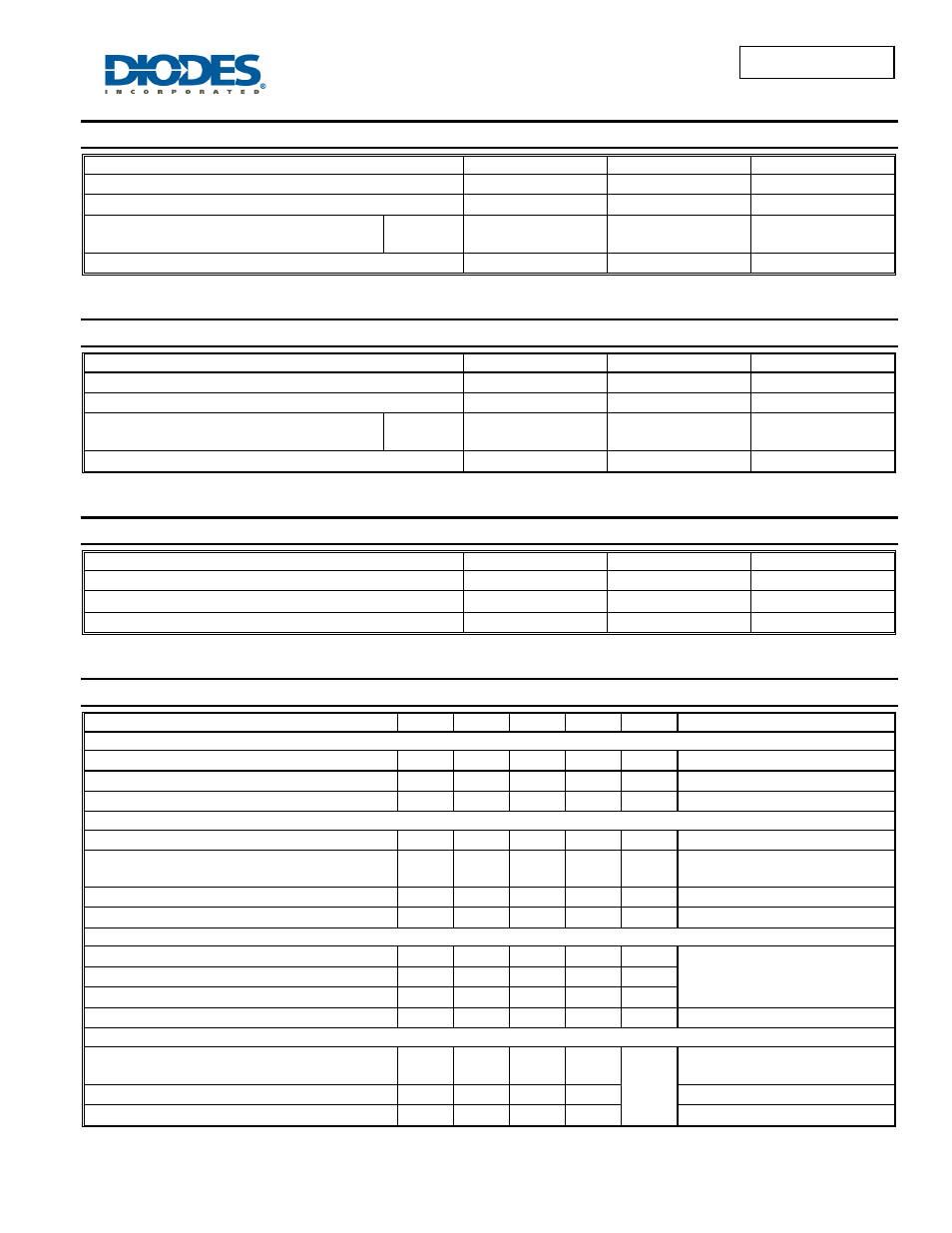
Maximum Ratings N-CHANNEL – Q2
(@T
A
= +25°C, unless otherwise specified.)
Characteristic Symbol
Value
Unit
Drain Source Voltage
V
DSS
30 V
Gate-Source Voltage
V
GSS
±20
V
Drain Current (Note 5)
T
A
= +25°C
T
A
= +70°C
I
D
9.1
7.7
A
Pulsed Drain Current (Note 6)
I
DM
32 A
Maximum Ratings P-CHANNEL – Q1
(@T
A
= +25°C, unless otherwise specified.)
Characteristic Symbol
Value
Unit
Drain Source Voltage
V
DSS
-30 V
Gate-Source Voltage
V
GSS
±20
V
Drain Current (Note 5)
T
A
= +25°C
T
A
= +70°C
I
D
-6
-5
A
Pulsed Drain Current (Note 6)
I
DM
-21 A
Thermal Characteristics
(@T
A
= +25°C, unless otherwise specified.)
Characteristic Symbol
Value
Unit
Power Dissipation (Note 5)
P
D
2.5 W
Thermal Resistance, Junction to Ambient
R
θJA
50
°C/W
Operating and Storage Temperature Range
T
J
, T
STG
-55 to +150
°C
Electrical Characteristics N-CHANNEL – Q2
(@T
A
= +25°C, unless otherwise specified.)
Characteristic Symbol
Min
Typ
Max
Unit
Test
Condition
OFF CHARACTERISTICS (Note 7)
Drain-Source Breakdown Voltage
BV
DSS
30
⎯
⎯
V
V
GS
= 0V, I
D
= 250µA
Zero Gate Voltage Drain Current
I
DSS
⎯
⎯
1 µA
V
DS
= 24V, V
GS
= 0V
Gate-Source Leakage
I
GSS
⎯
⎯
± 100
nA
V
GS
= ±20V, V
DS
= 0V
ON CHARACTERISTICS (Note 7)
Gate Threshold Voltage
V
GS(th)
1 1.9 2.1 V
V
DS
= V
GS
, I
D
= 250µA
Static Drain-Source On-Resistance
R
DS(ON)
⎯
⎯
18
29
20
32
m
Ω
V
GS
= 10V, I
D
= 6.9A
V
GS
= 4.5V, I
D
= 5.0A
Forward Transfer Admittance
|Y
fs
|
⎯
10
⎯
S
V
DS
= 5V, I
D
= 6.9A
Diode Forward Voltage (Note 7)
V
SD
0.5
⎯
1.2 V
V
GS
= 0V, I
S
= 1A
DYNAMIC CHARACTERISTICS
Input Capacitance
C
iss
⎯
631
⎯
pF
V
DS
= 15V, V
GS
= 0V, f =1.0MHz
Output Capacitance
C
oss
⎯
147
⎯
pF
Reverse Transfer Capacitance
C
rss
⎯
99
⎯
pF
Gate Resistance
R
G
⎯
0.9
⎯
Ω
V
DS
= 0V, V
GS
= 0V, f = 1.0MHz
SWITCHING CHARACTERISTICS
Total Gate Charge
Q
g
⎯
5.9
12.4
⎯
nC
V
DS
= 15V, V
GS
= 4.5V, I
D
= 7A
V
DS
= 15V, V
GS
= 10V, I
D
= 9A
Gate-Source Charge
Q
gs
⎯
1.8
⎯
V
DS
= 15V, V
GS
= 10V, I
D
= 9A
Gate-Drain Charge
Q
gd
⎯
3.4
⎯
V
DS
= 15V, V
GS
= 10V, I
D
= 9A
Notes:
5. Device mounted on FR-4 PCB, on 2oz. Copper pads with R
ΘJA
= 50°C/W
6. Repetitive rating, pulse width limited by junction temperature.
7. Short duration pulse test used to minimize self-heating effect.