Diodes DMC2004DWK User Manual
Dmc2004dwk new prod uc t, Features, Mechanical data
DMC2004DWK
Document number: DS31114 Rev. 4 - 2
1 of 8
www.diodes.com
September 2007
© Diodes Incorporated
DMC2004DWK
NEW PROD
UC
T
COMPLEMENTARY PAIR ENHANCEMENT MODE FIELD EFFECT TRANSISTOR
Features
•
Low On-Resistance
•
Low Gate Threshold Voltage V
GS(th)
< 1V
•
Low Input Capacitance
•
Fast Switching Speed
•
Low Input/Output Leakage
•
Complementary Pair MOSFET
•
Ultra-Small Surface Mount Package
•
Lead Free/RoHS Compliant (Note 2)
•
ESD Protected Gate
•
"Green" Device (Note 3)
Mechanical Data
•
Case: SOT-363
•
Case Material: Molded Plastic. UL Flammability Classification
Rating 94V-0
•
Moisture Sensitivity: Level 1 per J-STD-020C
•
Terminals: Solderable per MIL-STD-202, Method 208
•
Lead Free Plating (Matte Tin Finish annealed over Alloy 42
leadframe).
•
Terminal Connections: See Diagram
•
Marking Information: See Page 7
•
Ordering & Date Code Information: See Page 7
•
Weight: 0.006 grams (approximate)
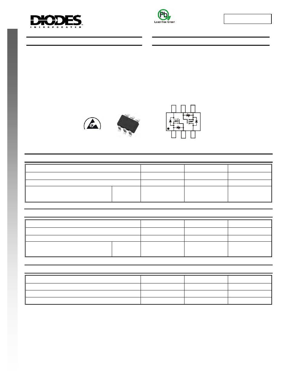
SOT-363
S
2
D
2
Q
1
Q
2
D
1
S
1
G
2
G
1
ESD protected
TOP VIEW
TOP VIEW
Internal Schematic
Maximum Ratings N-CHANNEL – Q
1
@T
A
= 25°C unless otherwise specified
Characteristic Symbol
Value
Unit
Drain Source Voltage
V
DSS
20 V
Gate-Source Voltage
V
GSS
±8
V
Drain Current (Note 1)
T
A
= 25°C
T
A
= 85°C
I
D
540
390
mA
Maximum Ratings P-CHANNEL – Q
2
@T
A
= 25°C unless otherwise specified
Characteristic Symbol
Value
Unit
Drain Source Voltage
V
DSS
-20 V
Gate-Source Voltage
V
GSS
±8
V
Drain Current (Note 1)
T
A
= 25°C
T
A
= 85°C
I
D
-430
-310
mA
Thermal Characteristics – Total Device
@T
A
= 25°C unless otherwise specified
Characteristic Symbol
Value
Unit
Power Dissipation (Note 1)
P
d
250 mW
Thermal Resistance, Junction to Ambient
R
θJA
500
°C/W
Operating and Storage Temperature Range
T
j
, T
STG
-65 to +150
°C
Notes:
1. Device mounted on FR-4 PCB.
2. No purposefully added lead.
3. Diodes Inc.’s “Green” policy can be found on our website at http://www.diodes.com/products/lead_free/index.php.