Maximum ratings, Thermal characteristics, Electrical characteristics – Diodes DMP6250SE User Manual
Page 2
DMP6250SE
Document Number DS36696 Rev. 1 - 2
2 of 6
January 2014
© Diodes Incorporated
DMP6250SE
ADVAN
CE I
N
F
O
RM
ATI
O
N
NEW PROD
UC
T
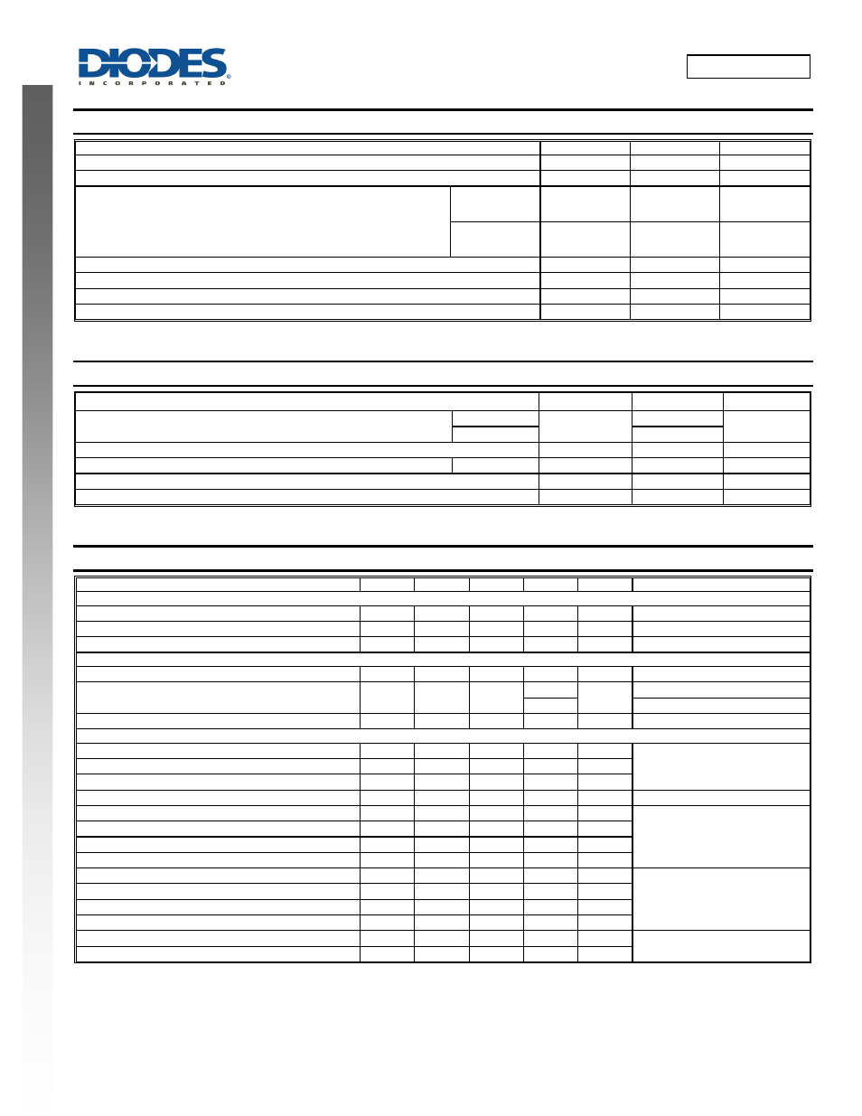
Maximum Ratings
(@T
A
= +25°C, unless otherwise specified.)
Characteristic Symbol
Value
Unit
Drain-Source voltage
V
DSS
-60 V
Gate-Source voltage (Note 5)
V
GS
±20
V
Continuous Drain current (Note 6) V
GS
= -10V
T
A
= +25°C
T
A
= +70°C
I
D
-2.1
-1.7
A
T
C
= +25°C
T
C
= +70°C
I
D
-6.1
-4.9
A
Maximum Body Diode Continuous Current
I
S
-1.8 A
Pulsed Drain Current (10µs pulse, duty cycle = 1%)
I
DM
-11 A
Single Pulsed Avalanche Current (Note 7) L = 0.1mH
I
AS
-12 A
Single Pulsed Avalanche Energy (Note 7) L = 0.1mH
E
AS
8 mJ
Thermal Characteristics
(@T
A
= +25°C, unless otherwise specified.)
Characteristic Symbol
Value
Units
Total Power Dissipation (Note 6)
T
A
= +25°C
P
D
1.8
W
T
A
= +70°C
1.1
Thermal Resistance, Junction to Ambient (Note 6)
R
θJA
69 °C/W
Total Power Dissipation (Note 6)
T
C
= +25°C
P
D
14
W
Thermal Resistance, Junction to Case (Note 6)
R
θJC
8.7
Operating and Storage Temperature Range
T
J,
T
STG
-55 to +150
°C
Electrical Characteristics
(@T
A
= +25°C, unless otherwise specified.)
Characteristic Symbol
Min
Typ
Max
Unit
Test
Condition
OFF CHARACTERISTICS (Note 8)
Drain-Source Breakdown Voltage
BV
DSS
-60
⎯
⎯
V
I
D
= -250µA, V
GS
= 0V
Zero Gate Voltage Drain Current
I
DSS
⎯
⎯
-1 µA
V
DS
= -60V, V
GS
= 0V
Gate-Source Leakage
I
GSS
⎯
⎯
±100
nA
V
GS
=
±20V, V
DS
= 0V
ON CHARACTERISTICS (Note 8)
Gate Threshold Voltage
V
GS(th)
-1
⎯
-3 V
V
DS
= V
GS
, I
D
= -250µA
Static Drain-Source On-Resistance
R
DS (ON)
⎯
⎯
250
mΩ
V
GS
= -10V, I
D
= -1.0A
300
V
GS
= -4.5V, I
D
= -0.5A
Diode Forward Voltage
V
SD
⎯
⎯
-1.2 V
V
GS
= 0V, I
S
= -2.0A
DYNAMIC CHARACTERISTICS (Note 9)
Input Capacitance
C
iss
⎯
551
⎯
pF
V
DS
= -30V, V
GS
= 0V
f= 1MHz
Output Capacitance
C
oss
⎯
25.7
⎯
pF
Reverse Transfer Capacitance
C
rss
⎯
19.1
⎯
pF
Gate Resistance
R
g
⎯
12.1
⎯
Ω
V
DS
= 0V, V
GS
= 0V, f = 1MHz
Total Gate Charge (VGS = -4.5V)
Q
g
⎯
4.8
⎯
nC
V
DS
= -30V, I
D
= -2A
Total Gate Charge (VGS = -10V)
Q
g
⎯
9.7
⎯
nC
Gate-Source Charge
Q
gs
⎯
1.5
⎯
nC
Gate-Drain Charge
Q
gd
⎯
1.6
⎯
nC
Turn-On Delay Time
t
D(on)
⎯
6.3
⎯
ns
V
DS
= -30V, V
GS
= -10V,
R
G
= 50Ω, I
D
= -1A
Turn-On Rise Time
t
r
⎯
10.3
⎯
ns
Turn-Off Delay Time
t
D(off)
⎯
91.4
⎯
ns
Turn-Off Fall Time
t
f
⎯
39.8
⎯
ns
Reverse recovery time
t
rr
9.2
⎯
ns
I
S
= -1A, di/dt= 100A/µs
Reverse recovery charge
Q
rr
⎯
3.9
⎯
nC
Notes:
5. AEC-Q101 V
GS
maximum is
±16V.
6. Device mounted on FR-4 substrate PC board, 2oz copper, with 1inch square copper plate.
7. IAR and EAR rating are based on low frequency and duty cycles to keep T
J
= 25°C
8. Short duration pulse test used to minimize self-heating effect.
9. For design aid only, not subject to production testing.