Maximum ratings, Thermal characteristics – Diodes DMP4025LK3 User Manual
Page 2
DMP4025LK3
Document Number:35938 Rev. 3 - 2
2 of 8
www.diodes.com
March 2014
© Diodes Incorporated
ADVAN
CE I
N
F
O
RM
ATI
O
N
DMP4025LK3
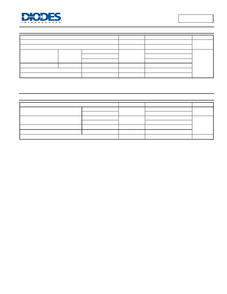
Maximum Ratings
(@T
A
= +25°C unless otherwise specified.)
Characteristic Symbol
Value
Units
Drain-Source Voltage
V
DSS
-40
V
Gate-Source Voltage
V
GSS
20
Continuous Drain Current
V
GS
= -10V
(Notes 6)
I
D
-8.6
A
T
A
= +70°C (Notes 6)
-6.9
(Notes 5)
-6.7
Pulsed Drain Current
V
GS
= -10V
(Notes 7)
I
DM
-35
Continuous Source Current (Body diode)
(Notes 7)
I
S
-8.6
Pulsed Source Current (Body diode)
(Notes 7)
I
SM
-35
Thermal Characteristics
(@T
A
= +25°C unless otherwise specified.)
Characteristic Symbol
Value
Unit
Power Dissipation
(Notes 5)
P
D
1.7
W
(Notes 6)
2.78
Thermal Resistance, Junction to Ambient
(Notes 5)
R
θJA
74
°C/W
(Notes 6)
45
Thermal Resistance, Junction to Case
(Notes 6)
R
θJC
7.1
Thermal Resistance, Junction to Lead
(Notes 8)
R
θJL
1.43
Operating and Storage Temperature Range
T
J,
T
STG
-55 to +150
°C
Notes:
5. For a device surface mounted on minimum recommended FR4 PCB with high coverage of single sided 1oz copper, in still air conditions; the device is
measured when operating in a steady-state condition.
6. Same as note (5), except the device is surface mounted on 25mm X 25mm X 1.6mm FR4 PCB.
7. Repetitive rating on 25mm X 25mm FR4 PCB, D=0.02, pulse width 300µs – pulse width by maximum junction temperature.
8. Thermal resistance from junction to solder-point (at the end of the drain lead).