Maximum ratings, Thermal characteristics, Dmp31d0ufb4 – Diodes DMP31D0UFB4 User Manual
Page 2: A product line of diodes incorporated
DMP31D0UFB4
D
atasheet number: DS35587 Rev. 1 - 2
2 of 7
January 2012
© Diodes Incorporated
A Product Line of
Diodes Incorporated
DMP31D0UFB4
Maximum Ratings
@T
A
= 25°C unless otherwise specified
Characteristic
Symbol
Value
Unit
Drain-Source Voltage
V
DSS
-30 V
Gate-Source Voltage
V
GSS
±8 V
Continuous Drain Current
Steady
State
T
A
= 25°C (Note 5)
T
A
= 85°C (Note 5)
T
A
= 25°C (Note 4)
I
D
-0.76
-0.55
-0.54
A
Pulsed Drain Current (Note 5)
I
DM
2 A
Thermal Characteristics
@T
A
= 25°C unless otherwise specified
Characteristic Symbol
Value
Unit
Power Dissipation
(Note 4)
P
D
0.46
W
(Note 5)
0.92
Thermal Resistance, Junction to Ambient
(Note 4)
R
θJA
271
°C/W
(Note 5)
136
Operating and Storage Temperature Range
T
J
,
T
STG
-55 to +150
°C
Notes:
4. Device mounted on FR-4 substrate PC board, 2oz copper, with minimum recommended pad layout
5. Device mounted on FR-4 substrate PC board, 2oz copper, with thermal vias to bottom layer 1inch square copper plate
6. Device mounted on minimum recommended pad layout test board, 10
μs pulse duty cycle = 1%.
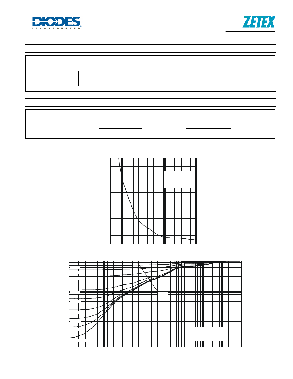
0
1
2
3
4
5
6
7
8
9
10
0.001
0.01
0.1
1
10
100
1,000
P
,
P
EAK
T
R
ANSI
E
N
T
P
O
IW
E
R
(W
)
(P
K
)
t1, PULSE DURATION TIME (sec)
Fig. 1 Single Pulse Maximum Power Dissipation
Single Pulse
R
= 262 C/W
R
= r
* R
T - T = P * R
θ
θ
θ
θ
JA
JA(t)
(t)
JA
J
A
JA(t)
°
0.000001 0.00001
0.0001
0.001
0.01
0.1
1
10
100
1,000
0.001
0.01
0.1
r(t),
T
R
ANSI
EN
T
T
H
E
R
MAL
R
ESI
S
T
AN
C
E
1
R
(t) = r(t) * R
θ
θ
JA
JA
R
= 262°C/W
Duty Cycle, D = t1/ t2
θJA
D = 0.7
D = 0.9
D = 0.5
D = 0.3
D = 0.1
D = 0.05
D = 0.02
D = 0.01
D = 0.005
Single Pulse
t1, PULSE DURATION TIMES (sec)
Fig. 2 Transient Thermal Resistance