Dmp3098ldm, Electrical characteristics, New prod uc t – Diodes DMP3098LDM User Manual
Page 2
DMP3098LDM
Electrical Characteristics
@T
A
= 25°C unless otherwise specified
Characteristic Symbol
Min
Typ
Max
Unit
Test
Condition
STATIC PARAMETERS
Drain-Source Breakdown Voltage
BV
DSS
-30
⎯
⎯
V
I
D
= -250
μA, V
GS
= 0V
I
DSS
⎯
⎯
-1
μA
V
DS
= -30V, V
GS
= 0V
Zero Gate Voltage Drain Current T
J
= 25
°C
Gate-Body Leakage Current
I
GSS
⎯
⎯
±100
nA
V
DS
= 0V, V
GS
=
±20V
NEW PROD
UC
T
Gate Threshold Voltage
V
GS(th)
-1.0
⎯
-2.1 V
V
DS
= V
GS
, I
D
= -250
μA
On State Drain Current (Note 5)
I
D (ON)
-15
⎯
⎯
A
V
GS
= -4.5V, V
DS
= -5V
R
DS (ON)
⎯
56
98
65
115
m
Ω
V
GS
= -10V, I
D
= -4.0A
V
GS
= -4.5V, I
D
= -3.0A
Static Drain-Source On-Resistance (Note 5)
Forward Transconductance (Note 5)
g
FS
⎯
5.3
⎯
S
V
DS
= -10V, I
D
= -4.0A
Diode Forward Voltage (Note 5)
V
SD
⎯
0.79 -1.2 V I
S
= -1.7A, V
GS
= 0V
DYNAMIC PARAMETERS (Note 6)
Input Capacitance
C
iss
⎯
336
⎯
pF
DMP3098LDM
Document number: DS31446 Rev. 3 - 2
2 of 4
www.diodes.com
October 2008
© Diodes Incorporated
Output Capacitance
C
oss
⎯
70
⎯
pF
C
rss
⎯
49
⎯
pF
V
DS
= -25V, V
GS
= 0V
f = 1.0MHz
Reverse Transfer Capacitance
Gate Resistance
R
G
⎯
4.6
⎯
Ω
V
DS
= 0V, V
GS
= 0V, f = 1.0MHz
SWITCHING CHARACTERISTICS
Q
g
⎯
4.0
7.8
⎯
V
DS
= -15V, V
GS
= -4.5V, I
D
= -5.0A
V
DS
= -15V, V
GS
= -10V, I
D
= -5.0A
Total Gate Charge
Gate-Source Charge
Q
gs
⎯
1.0
⎯
V
DS
= -15V, V
GS
= -4.5V, I
D
= -5.0A
Q
gd
⎯
2.5
⎯
nC
Gate-Drain Charge
V
DS
= -15V, V
GS
= -4.5V, I
D
= -5.0A
Turn-On Delay Time
t
d(on)
⎯
6.0
⎯
Rise Time
t
r
⎯
5.0
⎯
Turn-Off Delay Time
t
d(off)
⎯
17.6
⎯
t
f
⎯
9.5
⎯
ns
V
DS
= -15V, V
GS
= -10V,
I
D
= -1.0A, R
G
= 6.0
Ω
Fall Time
Notes:
5. Test pulse width t = 300
μs.
6. Guaranteed by design. Not subject to production testing.
-I
, D
RA
IN CU
RRENT
(
A
)
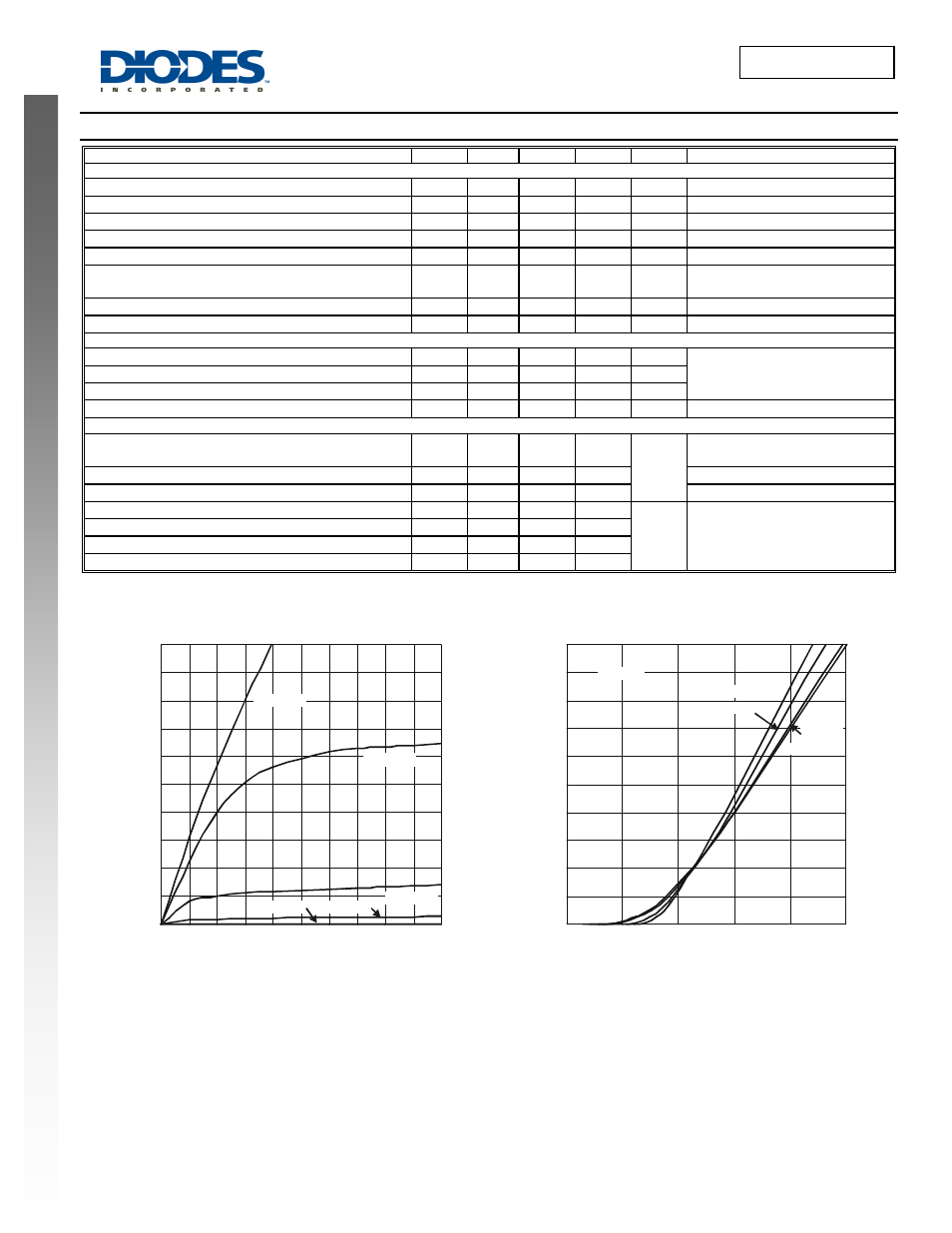
D
Fig. 1 Typical Output Characteristics
-V , DRAIN-SOURCE VOLTAGE (V)
DS
0
4
8
12
16
20
0
1
2
3
4
Fig. 2 Typical Transfer Characteristics
-V , GATE SOURCE VOLTAGE (V)
GS
-I
, D
R
AI
N
C
U
R
R
E
N
T
(A
)
D
0
4
8
12
16
20
1
2
3
4
5
6
V
= -5V
DS
T = -55°C
A
T = 25°C
A
T = 125°C
A
T = 150°C
A
5
V
= -2.5V
GS
V
= -4.5V
GS
V
= -10V
GS
V
= -1.5V
GS
V
= -3.0V
GS