Electrical characteristics, Dmp3017sfg – Diodes DMP3017SFG User Manual
Page 3
POWERDI is a registered trademark of Diodes Incorporated
DMP3017SFG
Document number: DS36479 Rev. 3 - 2
3 of 7
December 2013
© Diodes Incorporated
DMP3017SFG
ADVAN
CE I
N
F
O
RM
ATI
O
N
Electrical Characteristics
(@T
A
= +25°C, unless otherwise specified.)
Characteristic
Symbol
Min
Typ
Max
Unit
Test Condition
OFF CHARACTERISTICS (Note 8)
Drain-Source Breakdown Voltage
BV
DSS
-30
—
— V
V
GS
= 0V, I
D
= -250μA
Zero Gate Voltage Drain Current
I
DSS
—
—
-1
μA
V
DS
= -24V, V
GS
= 0V
Gate-Source Leakage
I
GSS
—
—
±10
μA
V
GS
= ±25V, V
DS
= 0V
ON CHARACTERISTICS (Note 8)
Gate Threshold Voltage
V
GS(th)
-1.0 — -3.0 V
V
DS
= V
GS
, I
D
= -250μA
Static Drain-Source On-Resistance
R
DS (ON)
—
8.5 10
mΩ
V
GS
= -10V, I
D
= -11.5A
—
15 18
V
GS
= -4.5V, I
D
= -8.5A
Forward Transfer Admittance
|Y
fs
|
—
24 — S
V
DS
= -5V, I
D
= -11.5A
DYNAMIC CHARACTERISTICS (Note 9)
Input Capacitance
C
iss
—
2246 — pF
V
DS
= -15V, V
GS
= 0V,
f = 1.0MHz
Output Capacitance
C
oss
—
352 — pF
Reverse Transfer Capacitance
C
rss
—
294 — pF
Gate resistance
R
g
—
5.1 12 Ω
V
DS
= 0V, V
GS
= 0V, f = 1.0MHz
Total Gate Charge (V
GS
= 5V)
Q
g
—
20.5 — nC
V
DS
= -15V, I
D
= -11.5A
Total Gate Charge (V
GS
= 10V)
Q
g
—
41 — nC
Gate-Source Charge
Q
gs
—
7.6 — nC
Gate-Drain Charge
Q
gd
—
8.0 — nC
Turn-On Delay Time
t
D(on)
—
7.5 — ns
V
DD
= -15V, V
GS
= -10V,
R
G
= 6Ω, I
D
= -11.5A
Turn-On Rise Time
t
r
—
15.4 — ns
Turn-Off Delay Time
t
D(off)
—
45.6 — ns
Turn-Off Fall Time
t
f
—
36.8 — ns
BODY DIODE CHARACTERISTICS
Diode Forward Voltage
V
SD
—
-0.7 — V
V
GS
= 0V, I
S
= -1A
Reverse Recovery Time (Note 9)
t
rr
—
20 — ns
I
S
= -11.5A, dI/dt = 100A/μs
Reverse Recovery Charge (Note 9)
Q
rr
—
9.5 — nC
Notes:
5. Device mounted on FR-4 substrate PC board, 2oz copper, with minimum recommended pad layout.
6. Device mounted on FR-4 substrate PC board, 2oz copper, with 1inch square copper plate.
7. I
AR
and E
AR
rating are based on low frequency and duty cycles to keep T
J
= +25°C
8. Short duration pulse test used to minimize self-heating effect.
9. Guaranteed by design. Not subject to product testing.
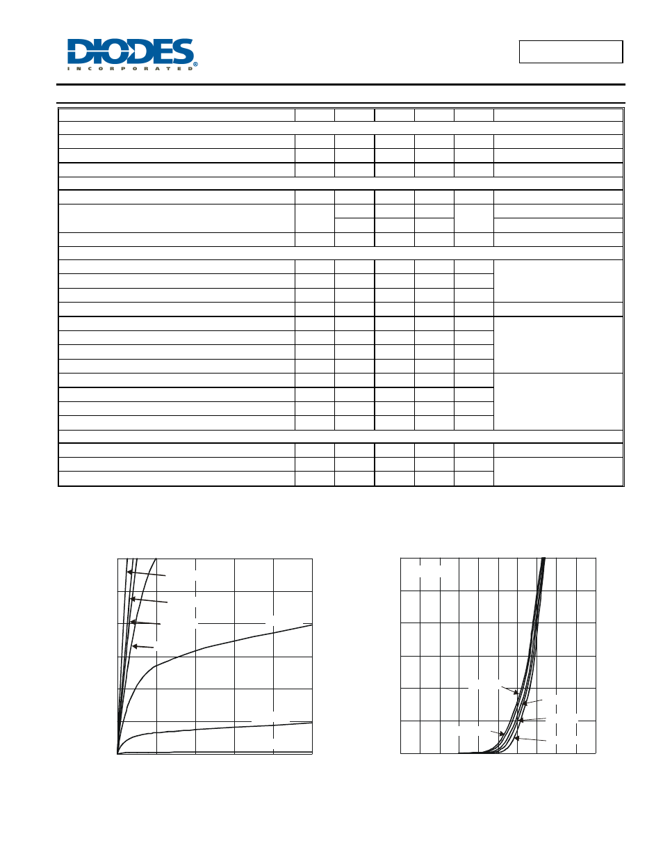
-V , DRAIN -SOURCE VOLTAGE (V)
Figure 1 Typical Output Characteristics
DS
-I
, D
R
AI
N
C
U
R
R
EN
T
(A
)
D
0.0
5.0
10.0
15.0
20.0
25.0
30.0
0
1
2
3
4
5
V
= -2.5V
GS
V
= -3.0V
GS
V
= -3.5V
GS
V
= -4.0V
GS
V
= -10V
GS
V
= -5.5V
GS
V
= -5.5V
GS
-V , GATE-SOURCE VOLTAGE (V)
GS
Figure 2 Typical Transfer Characteristics
-I
, D
R
AI
N
C
U
R
R
ENT (
A
)
D
0
5
10
15
20
25
30
0
0.5
1
1.5
2
2.5
3
3.5
4
4.5
5
T = 150°C
A
T = 125°C
A
T = 85°C
A
T = 25°C
A
T = -55°C
A
V
= -5.0V
DS