Maximum ratings, Thermal characteristics, Electrical characteristics – Diodes DMP3010LK3 User Manual
Page 2
DMP3010LK3
Document number: DS35716 Rev. 4 - 2
2 of 7
February 2012
© Diodes Incorporated
DMP3010LK3
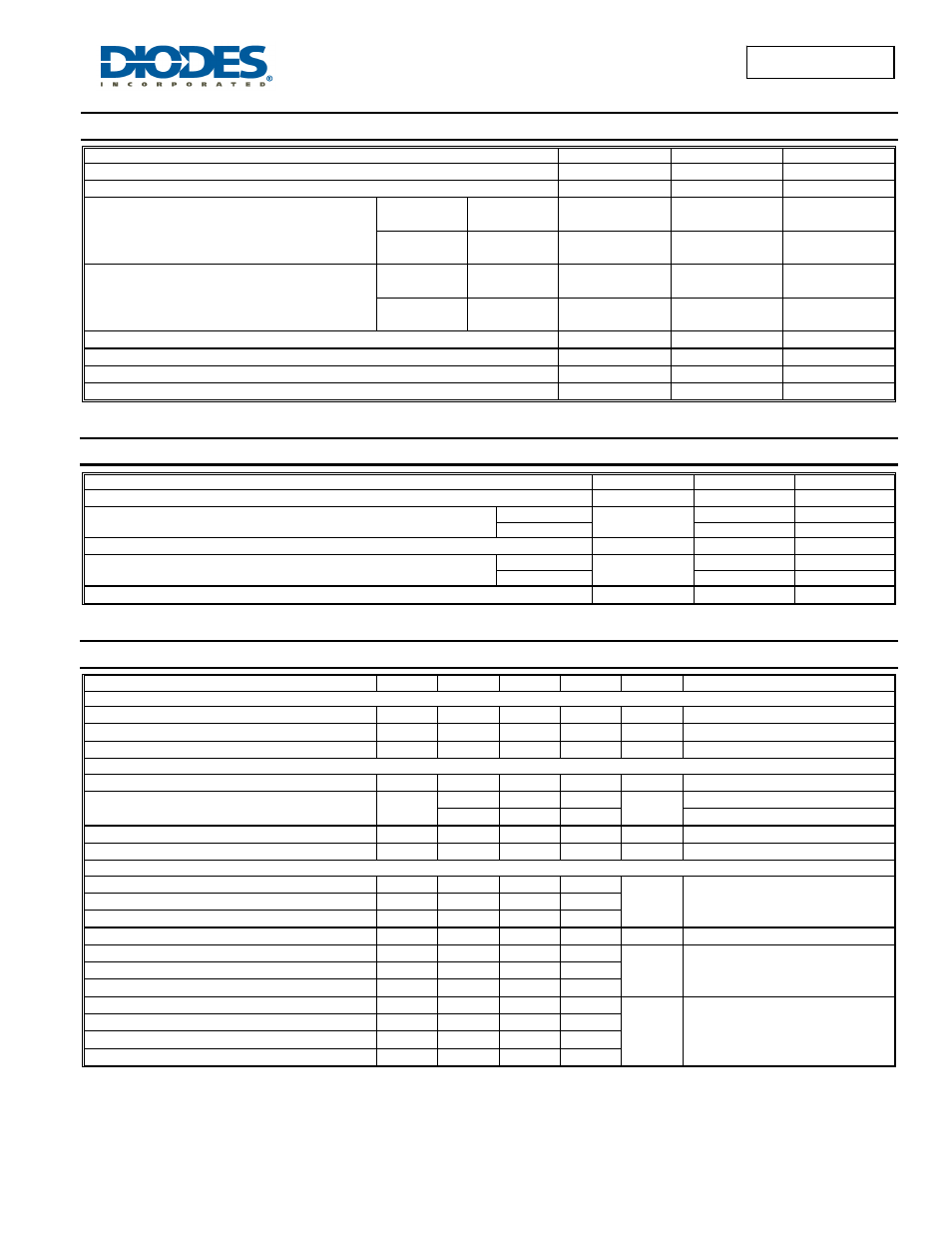
Maximum Ratings
@T
A
= 25°C unless otherwise specified
Characteristic Symbol
Value
Units
Drain-Source Voltage
V
DSS
-30 V
Gate-Source Voltage
V
GSS
±20 V
Continuous Drain Current (Note 4) V
GS
= -10V
Steady
State
T
A
= 25°C
T
A
= 70°C
I
D
-17.0
-13.0
A
t<10s
T
A
= 25°C
T
A
= 70°C
I
D
-27.0
-21.0
A
Continuous Drain Current (Note 4) V
GS
= -4.5V
Steady
State
T
A
= 25°C
T
A
= 70°C
I
D
-14.5
-11.5
A
t<10s
T
A
= 25°C
T
A
= 70°C
I
D
-23.0
-18.0
A
Pulsed Drain Current (10
μs pulse, duty cycle = 1%)
I
DM
-100 A
Maximum Body Diode Forward Current (Note 4)
I
S
5.5 A
Avalanche Current (Note 5)
I
AS
47 A
Avalanche Energy (Note 5)
E
AS
113 mJ
Thermal Characteristics
@T
A
= 25°C unless otherwise specified
Characteristic Symbol
Value
Units
Total Power Dissipation (Note 3)
P
D
1.7 W
Thermal Resistance, Junction to Ambient (Note 3)
Steady state
R
θJA
72 °C/W
t<10s 29
°C/W
Total Power Dissipation (Note 4)
P
D
3.4 W
Thermal Resistance, Junction to Ambient (Note 4)
Steady state
R
θJA
37 °C/W
t<10s 15
°C/W
Operating and Storage Temperature Range
T
J,
T
STG
-55 to +150
°C
Electrical Characteristics
@T
A
= 25°C unless otherwise specified
Characteristic Symbol
Min
Typ
Max
Unit
Test
Condition
OFF CHARACTERISTICS (Note 6)
Drain-Source Breakdown Voltage
BV
DSS
-30
⎯
⎯
V
V
GS
= 0V, I
D
= -250
μA
Zero Gate Voltage Drain Current
I
DSS
⎯
⎯
-1
µA
V
DS
= -30V, V
GS
= 0V
Gate-Source Leakage
I
GSS
⎯
⎯
±100
nA
V
GS
=
±20V, V
DS
= 0V
ON CHARACTERISTICS (Note 6)
Gate Threshold Voltage
V
GS(th)
-1.1 -1.6 -2.1 V
V
DS
= V
GS
, I
D
= -250
μA
Static Drain-Source On-Resistance
R
DS (ON)
⎯
6.5 8
m
Ω
V
GS
= -10V, I
D
= -10A
⎯
7.2 10.2
V
GS
= -4.5V, I
D
= -10A
Forward Transfer Admittance
|Y
fs
|
⎯
30
⎯
S
V
DS
= -15V, I
D
= -10A
Diode Forward Voltage
V
SD
⎯
-0.65 -1.0 V
V
GS
= 0V, I
S
= -1A
DYNAMIC CHARACTERISTICS (Note 7)
Input Capacitance
C
iss
⎯
6234
⎯
pF
V
DS
= 15V, V
GS
= 0V
f = 1.0MHz
Output Capacitance
C
oss
⎯
1500
⎯
Reverse Transfer Capacitance
C
rss
⎯
774
⎯
Gate Resistance
R
G
⎯
1.28
⎯
Ω
V
DS
= 0V, V
GS
= 0V, f = 1.0MHz
Total Gate Charge
Q
g
⎯
59.2
⎯
nC
V
DS
= -15V, V
GS
= -4.5V,
I
D
= -10A
Gate-Source Charge
Q
gs
⎯
16.1
⎯
Gate-Drain Charge
Q
gd
⎯
15.7
⎯
Turn-On Delay Time
t
D(on)
⎯
11.4
⎯
ns
V
DS
= -15V, V
GEN
= -10V,
R
G
= 6
Ω, I
D
= -1A
Turn-On Rise Time
t
r
⎯
9.4
⎯
Turn-Off Delay Time
t
D(off)
⎯
260.7
⎯
Turn-Off Fall Time
t
f
⎯
99.3
⎯
Notes:
3. Device mounted on FR-4 PC board, with minimum recommended pad layout, single sided.
4. Device mounted on FR-4 substrate PC board, 2oz copper, with thermal bias to bottom layer 1inch square copper plate
5 .UIS in production with L = 0.1mH, T
J
= 25°C
6. Short duration pulse test used to minimize self-heating effect.
7. Guaranteed by design. Not subject to production testing.