Dmg4435sss new prod uc t, Maximum ratings, Thermal characteristics – Diodes DMG4435SSS User Manual
Page 2: Electrical characteristics, Dmg4435sss
DMG4435SSS
Document number: DS32041 Rev. 5 - 2
2 of 6
September 2013
© Diodes Incorporated
DMG4435SSS
NEW PROD
UC
T
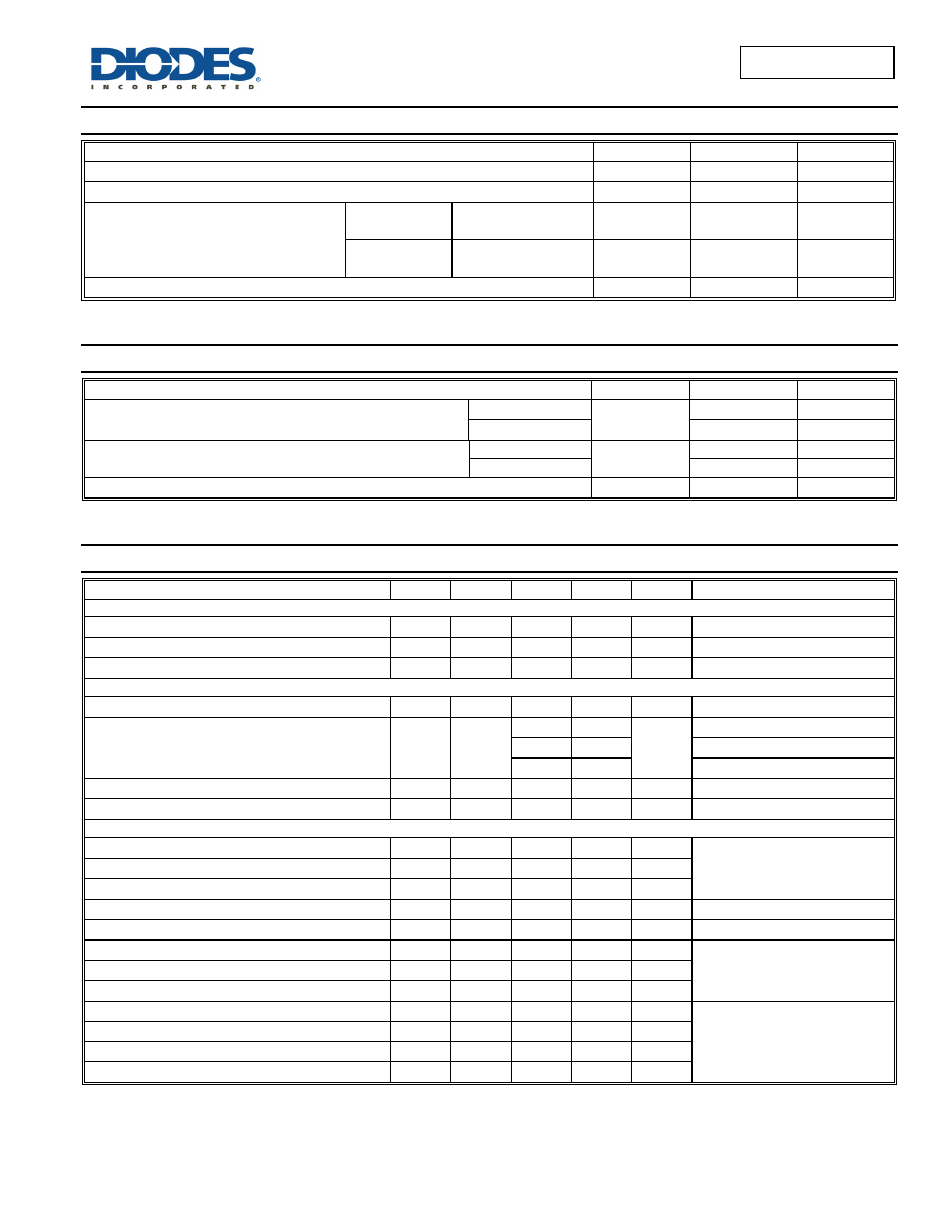
Maximum Ratings
(@T
A
= +25°C, unless otherwise specified.)
Characteristic
Symbol
Value
Unit
Drain-Source Voltage
V
DSS
-30 V
Gate-Source Voltage
V
GSS
±25 V
Continuous Drain Current (Note 5) V
GS
= -20
Steady State
T
A
= +25°C
T
A
= +70°C
I
D
-7.3
-5.7
A
t < 10s
T
A
= +25°C
T
A
= +70°C
I
D
-10
-7.5
A
Pulsed Drain Current (Note 6)
I
DM
-80 A
Thermal Characteristics
Characteristic Symbol
Value
Unit
Power Dissipation (Note 5)
T
A
= +25°C
P
D
2.5 W
T
A
= +70°C
1.5 W
Thermal Resistance, Junction to Ambient @T
A
= +25°C
Steady state
R
θJA
96.5 °C/W
t < 10s
55
°C/W
Operating and Storage Temperature Range
T
J
,
T
STG
-55 to +150
°C
Electrical Characteristics
(@T
A
= +25°C, unless otherwise specified.)
Characteristic
Symbol
Min
Typ
Max
Unit
Test Condition
OFF CHARACTERISTICS (Note 7)
Drain-Source Breakdown Voltage
BV
DSS
-30
—
— V
V
GS
= 0V, I
D
= -1mA
Zero Gate Voltage Drain Current T
J
= +25°C
I
DSS
—
—
-1.0 µA
V
DS
= -30V, V
GS
= 0V
Gate-Source Leakage
I
GSS
—
—
±100 nA
V
GS
= ±25V, V
DS
= 0V
ON CHARACTERISTICS (Note 7)
Gate Threshold Voltage
V
GS(th)
-1.0 -1.7 -2.5 V
V
DS
= V
GS
, I
D
= -250μA
Static Drain-Source On-Resistance
R
DS (ON)
—
13 16
mΩ
V
GS
= -20V, I
D
= -11A
15 20
V
GS
= -10V, I
D
= -10A
21 29
V
GS
= -5V, I
D
= -5A
Forward Transfer Admittance
|Y
fs
|
—
22 — S
V
DS
= -5V, I
D
= -10A
Diode Forward Voltage
V
SD
—
-0.74 -1.0 V V
GS
= 0V, I
S
= -1A
DYNAMIC CHARACTERISTICS (Note 8)
Input Capacitance
C
iss
—
1614 —
pF
V
DS
= -15V, V
GS
= 0V,
f = 1.0MHz
Output Capacitance
C
oss
—
226
—
pF
Reverse Transfer Capacitance
C
rss
—
214
—
pF
Gate Resistance
R
g
—
6.8
—
Ω
V
DS
= 0V, V
GS
= 0V, f = 1MHz
Total Gate Charge at 10V
Q
g
—
35.4 —
nC
V
GS
= -10V, V
DS
= -15V, I
D
= -10A
Total Gate Charge at 5V
Q
g
—
18.9
—
nC
V
GS
= -5V, V
DS
= -15V,
I
D
= -10A
Gate-Source Charge
Q
gs
—
4.6
—
nC
Gate-Drain Charge
Q
gd
—
5.7 —
nC
Turn-On Delay Time
t
D(on)
—
8.6
—
ns
V
DS
= -15V, V
GS
= -10V,
R
L
= 1.5Ω, R
GEN
= 3Ω,
Turn-On Rise Time
t
r
—
12.7
—
ns
Turn-Off Delay Time
t
D(off)
—
44.9 —
ns
Turn-Off Fall Time
t
f
—
22.8
—
ns
Notes:
5. Device mounted on 1in. x 1in. FR-4 PCB with 2oz. Copper, and
the testing is based on the
t<10s.
The value in any given application depends on the
user’s specific board design.
6. Repetitive rating, pulse width limited by junction temperature.
7. Short duration pulse test used to minimize self-heating effect.
8. Guaranteed by design. Not subject to production testing.