Package outline dimensions, Suggested pad layout – Diodes DMP2200UFCL User Manual
Page 5
DMP2200UFCL
Document number: DS36619 Rev. 2 - 2
5 of 6
June 2014
© Diodes Incorporated
DMP2200UFCL
ADVAN
CE I
N
F
O
RM
ATI
O
N
NEW PROD
UC
T
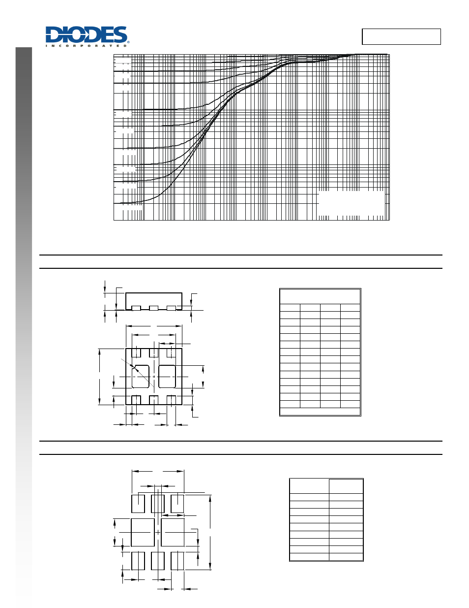
t1, PULSE DURATION TIMES (sec)
Figure 13 Transient Thermal Resistance
r(t),
T
R
A
N
SI
E
N
T
T
H
E
R
MA
L
R
ESI
S
TA
N
C
E
R
(t) = r(t) * R
R
= 190°C/W
Duty Cycle, D = t1/ t2
θ
θ
θ
JA
JA
JA
D = 0.7
D = 0.9
D = 0.5
D = 0.3
D = 0.1
D = 0.05
D = 0.02
D = 0.01
D = 0.005
Single Pulse
0.001
0.01
0.1
1
0.000001 0.00001
0.0001
0.001
0.01
0.1
1
10
100
1000
Package Outline Dimensions
rsion.
Suggested Pad Layout
rsion.
U-DFN1616-6
Type F
Dim
Min
Max Typ
A
0.45 0.55 0.50
A1
0 0.05
0.02
A3
— —
0.127
b
0.20 0.30 0.25
D
1.55 1.65 1.60
D1
1.14 1.34 1.24
D2
0.38 0.58 0.48
E
1.55 1.65 1.60
E2
0.54 0.74 0.64
e
— — 0.50
K
— — 0.23
L
0.15 0.35 0.25
Z
— —
0.175
All Dimensions in mm
Dimensions
Value
(in mm)
C
0.500
G
0.150
G1
0.180
X
0.320
X1
0.580
X2
1.320
Y
0.450
Y1
0.700
Y
1.900
P i n # 1 I D
D 2 ︵2 X ︶
D 1
R 0 .
1 0 0
K
D
E
e
b
L
A
A 1
A 3
E 2 ︵2 x ︶
Z ︵4 x ︶
S e a t i n g P l a n e
Y 2
X 2
Y
C
X
Y 1
G
X 1
G 1