Maximum ratings, Thermal characteristics, Electrical characteristics – Diodes DMP2200UFCL User Manual
Page 2
DMP2200UFCL
Document number: DS36619 Rev. 2 - 2
2 of 6
June 2014
© Diodes Incorporated
DMP2200UFCL
ADVAN
CE I
N
F
O
RM
ATI
O
N
NEW PROD
UC
T
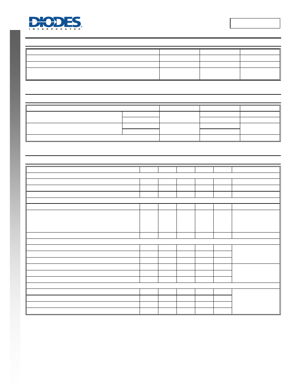
Maximum Ratings
(@T
A
= +25°C, unless otherwise specified.)
Characteristic Symbol
Value
Units
Drain-Source Voltage
V
DSS
-20 V
Gate-Source Voltage
V
GSS
±8 V
Continuous Drain Current (Note 6)
@T
A
= +25°C
@T
A
= +85°C
I
D
-1.7
-1.2
A
Thermal Characteristics
(@T
A
= +25°C, unless otherwise specified.)
Characteristic Symbol
Value
Units
Total Power Dissipation
(Note 5)
P
D
0.66 W
(Note 6)
1.58
W
Thermal Resistance, Junction to Ambient
(Note 5)
R
θJA
193
°C/W
(Note 6)
80
Operating and Storage Temperature Range
T
J,
T
STG
-55 to +150
°C
Electrical Characteristics
(@T
A
= +25°C, unless otherwise specified.)
Characteristic Symbol
Min
Typ
Max
Unit
Test
Condition
OFF CHARACTERISTICS (Note 7)
Drain-Source Breakdown Voltage
BV
DSS
-20
⎯
⎯
V
V
GS
= 0V, I
D
= 250µA
Zero Gate Voltage Drain Current
I
DSS
⎯
⎯
-1 µA
V
DS
= -20V, V
GS
= 0V
Gate-Body Leakage
I
GSS
⎯
⎯
±10
µA
V
GS
=
±8V, V
DS
= 0V
ON CHARACTERISTICS (Note 7)
Gate Threshold Voltage
V
GS(th)
-0.4
⎯
-1.2 V
V
DS
= V
GS
, I
D
= -250µA
Static Drain-Source On-Resistance
R
DS (ON)
⎯
153
220
260
360
200
290
390
650
m
Ω
V
GS
= -4.5V, I
D
= -2.0A
V
GS
= -2.5V, I
D
= -1.2A
V
GS
= -1.8V, I
D
= -0.24A
V
GS
= -1.5V, I
D
= -0.18A
Diode Forward Voltage (Note 7)
V
SD
⎯
⎯
-1.2 V
V
GS
= 0V, I
S
= -0.6A
DYNAMIC CHARACTERISTICS (Note 8)
Input Capacitance
C
iss
— 184 —
pF
V
DS
= -10V, V
GS
= 0V
f
= 1.0MHz
Output Capacitance
C
oss
—
25.8
—
pF
Reverse Transfer Capacitance
C
rss
—
18.6
—
pF
Total Gate Charge
Q
g
—
2.2 —
nC
V
GS
= -4.5V, V
DS
= -10V,
I
D
= -1.7A
Gate-Source Charge
Q
gs
—
0.4
—
nC
Gate-Drain Charge
Q
gd
—
0.5
—
nC
SWITCHING CHARACTERISTICS (Note 8)
Turn-On Delay Time
t
D(ON)
—
9.8 —
ns
V
DD
= -10V, I
D
= -1.5A,
V
GS
= -4.5V, R
GEN
= 1
Ω
Turn-Off Delay Time
t
D(OFF)
—
23
—
ns
Turn-On Rise Time
t
r
—
87
—
ns
Turn-Off Fall Time
t
f
—
41 —
ns
Notes:
5. Device mounted on FR-4 substrate PC board, 2oz copper, with minimum recommended pad layout.
6. Device mounted on FR-4 substrate PC board, 2oz copper, with 1inch square copper plate.
7. Short duration pulse test used to minimize self-heating effect.
8. Guaranteed by design. Not subject to product testing.