Electrical characteristics, Typical characteristics, Dmp21d0ufb4 – Diodes DMP21D0UFB4 User Manual
Page 3: A product line of diodes incorporated
DMP21D0UFB4
D
atasheet number: DS35279 Rev. 3 - 2
3 of 7
February 2012
© Diodes Incorporated
DMP21D0UFB4
A Product Line of
Diodes Incorporated
Electrical Characteristics
@T
A
= 25°C unless otherwise specified
Characteristic
Symbol
Min
Typ
Max
Unit
Test Condition
OFF CHARACTERISTICS (Note 7)
Drain-Source Breakdown Voltage
BV
DSS
20 - - V
V
GS
= 0V, I
D
= -250
μA
Zero Gate Voltage Drain Current T
J
= 25°C
I
DSS
- - -1
μA
V
DS
= -20V, V
GS
= 0V
Gate-Source Leakage
I
GSS
- -
±10
μA
V
GS
= ±8V, V
DS
= 0V
ON CHARACTERISTICS (Note 7)
Gate Threshold Voltage
V
GS(th)
- -0.7 - V
V
DS
= V
GS
, I
D
= -250
μA
Static Drain-Source On-Resistance
R
DS (ON)
- -
495
m
Ω
V
GS
= -4.5V, I
D
= -400mA
690
V
GS
= -2.5V, I
D
= -300mA
960
V
GS
= -1.8V, I
D
= -100mA
Forward Transfer Admittance
|Y
fs
|
50 - - mS
V
DS
= -3V, I
D
= -300mA
Diode Forward Voltage
V
SD
- -
-1.2
V
V
GS
= 0V, I
S
= -300mA
DYNAMIC CHARACTERISTICS
Input Capacitance
C
iss
- 76.5 - pF
V
DS
= -10V, V
GS
= 0V,
f = 1.0MHz
Output Capacitance
C
oss
- 13.7 - pF
Reverse Transfer Capacitance
C
rss
- 10.7 - pF
Gate Resistance
R
g
- 195 -
Ω
V
DS
= 0V, V
GS
= 0V, f = 1MHz
Total Gate Charge
Q
g
1.5 - nC
V
GS
= -8V, V
DS
= -15V, I
D
= -1A
Total Gate Charge
Q
g
- 1.0 - nC
V
GS
= -4.5V, V
DS
= -15V,
I
D
= -1A
Gate-Source Charge
Q
gs
- 0.2 - nC
Gate-Drain Charge
Q
gd
- 0.3 - nC
Turn-On Delay Time
t
D(on)
- 7.1 - ns
V
DS
= -10V, -I
D
= 1A
V
GS
= -4.5V, R
G
= 6
Ω
Turn-On Rise Time
t
r
- 8.0 - ns
Turn-Off Delay Time
t
D(off)
- 31.7 - ns
Turn-Off Fall Time
t
f
- 18.5 - ns
Notes:
4. Device mounted on FR-4 substrate PC board, 2oz copper, with minimum recommended pad layout
5. Device mounted on FR-4 substrate PC board, 2oz copper, with thermal vias to bottom layer 1inch square copper plate
6. Device mounted on minimum recommended pad layout test board, 10
μs pulse duty cycle = 1%.
7. Short duration pulse test used to minimize self-heating effect.
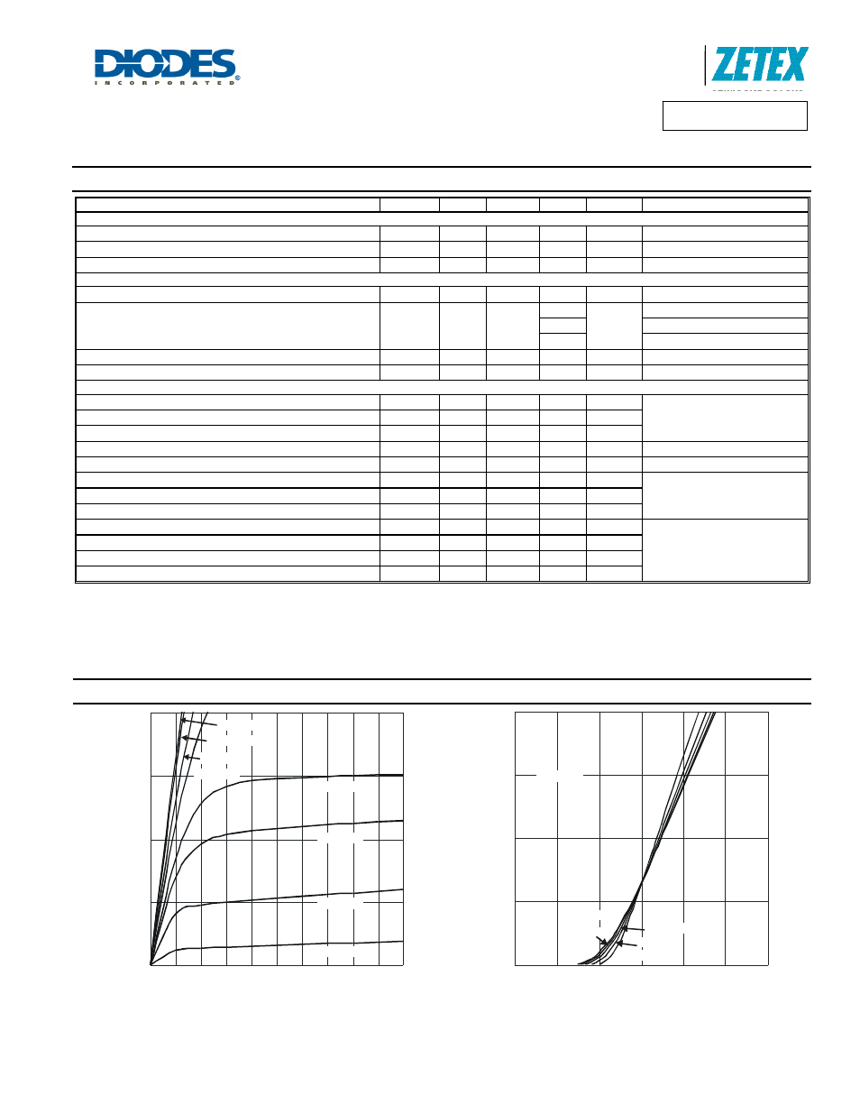
Typical Characteristics
0
0.5
1.0
1.5
2.0
0
1
2
3
4
5
Fig. 3 Typical Output Characteristic
-V
, DRAIN-SOURCE VOLTAGE (V)
DS
-I
, D
R
AI
N
C
U
R
R
EN
T
(A
)
D
V
= -1.2V
GS
V
= -1.5V
GS
V
= -2.0V
GS
V
= -2.5V
GS
V
= -3.0V
GS
V
= -4.5V
GS
V
= -4.0V
GS
V
= -1.8V
GS
0
0.5
1.0
1.5
2.0
0
0.5
1.0
1.5
2.0
2.5
3.0
-I
, D
R
AI
N
C
U
R
R
E
N
T
(A
)
D
Fig. 4 Typical Transfer Characteristic
-V
, GATE-SOURCE VOLTAGE (V)
GS
T = -55°C
A
T = 25°C
A
T = 85°C
A
T = 125°C
A
T = 150°C
A
V
= -5V
DS