Maximum ratings, Thermal characteristics, Electrical characteristics – Diodes DMP2070UCB6 User Manual
Page 2
DMP2070UCB6
Document number: DS35553 Rev. 2 - 2
2 of 6
October 2011
© Diodes Incorporated
DMP2070UCB6
NEW PROD
UC
T
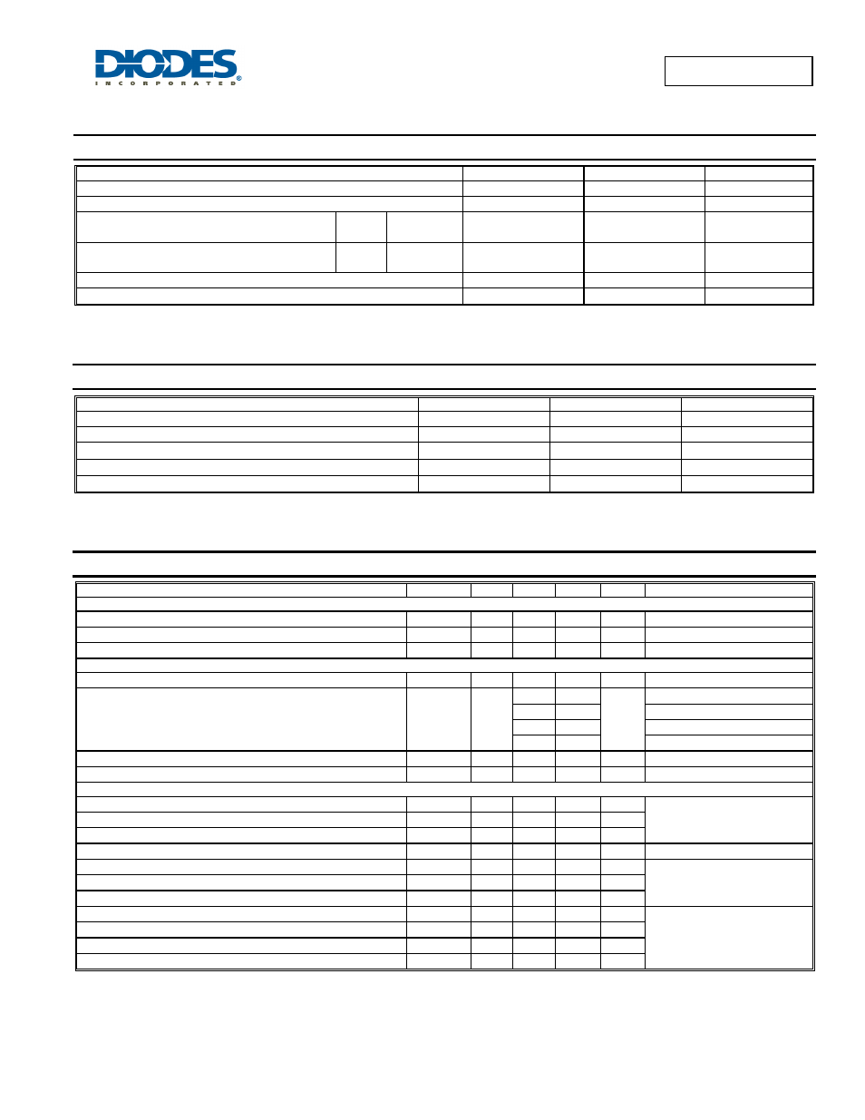
Maximum Ratings
@T
A
= 25°C unless otherwise specified
Characteristic Symbol
Value
Units
Drain-Source Voltage
V
DSS
-20 V
Gate-Source Voltage
V
GSS
±8 V
Continuous Drain Current (Note 4) V
GS
= -4.5V
Steady
State
T
A
= 25
°C
T
A
= 70
°C
I
D
-2.5
-2.0
A
Continuous Drain Current (Note 5) V
GS
= -4.5V
Steady
State
T
A
= 25
°C
T
A
= 70
°C
I
D
-3.5
-2.8
A
Pulsed Drain Current (Note 6)
I
DM
-12 A
Maximum Continuous Body Diode Forward Current (Note 5)
I
S
-1.8 A
Thermal Characteristics
@T
A
= 25°C unless otherwise specified
Characteristic Symbol
Value
Units
Total Power Dissipation (Note 4)
P
D
0.92 W
Total Power Dissipation (Note 5)
P
D
1.47 W
Thermal Resistance, Junction to Ambient (Note 4)
R
θJA
136 °C/W
Thermal Resistance, Junction to Ambient (Note 5)
R
θJA
84 °C/W
Operating and Storage Temperature Range
T
J,
T
STG
-55 to +150
°C
Electrical Characteristics
@T
A
= 25°C unless otherwise specified
Characteristic
Symbol
Min
Typ
Max
Unit
Test Condition
OFF CHARACTERISTICS (Note 7)
Drain-Source Breakdown Voltage
BV
DSS
-20 - - V
V
GS
= 0V, I
D
= -250
μA
Zero Gate Voltage Drain Current @T
C
= 25°C
I
DSS
- - -1
μA
V
DS
= -16V, V
GS
= 0V
Gate-Source Leakage
I
GSS
- -
±100
nA
V
GS
= ±8V, V
DS
= 0V
ON CHARACTERISTICS (Note 7)
Gate Threshold Voltage
V
GS(th)
-0.4 -0.6 -1.0 V V
DS
= V
GS
, I
D
= -250
μA
Static Drain-Source On-Resistance
R
DS (ON)
-
55 70
mΩ
V
GS
= -4.5V, I
D
= - 1A
70 90
V
GS
= -2.5V, I
D
= -1A
90 110
V
GS
= -1.8V, I
D
= -1A
110 150
V
GS
= -1.5V, I
D
= -1A
Forward Transfer Admittance
|Y
fs
|
- 12 - S
V
DS
= -10V, I
D
= -1A
Diode Forward Voltage (Note 5)
V
SD
- -0.7 -1 V
V
GS
= 0V, I
S
= -1A
DYNAMIC CHARACTERISTICS (Note 8)
Input Capacitance
C
iss
- 210 - pF
V
DS
= -10V, V
GS
= 0V,
f = 1.0MHz
Output Capacitance
C
oss
- 92 - pF
Reverse Transfer Capacitance
C
rss
- 38 - pF
Series Gate Resistance
R
G
5.3 - Ω
V
DS
= 0V, V
GS
= 0V, f = 1MHz
Total Gate Charge (4.5V)
Q
g
- 2.9 - nC
V
GS
= -4.5V, V
DS
= -10V,
I
D
= -1A ,
Gate-Source Charge
Q
gs
- 0.3 - nC
Gate-Drain Charge
Q
gd
- 0.5 - nC
Turn-On Delay Time
t
D(on)
- 7.3 - ns
V
DD
= -10V, V
GS
= -4.5V,
I
DS
= -1A, R
G
= 20
Ω,
Turn-On Rise Time
t
r
- 14.0 - ns
Turn-Off Delay Time
t
D(off)
- 42.6 - ns
Turn-Off Fall Time
t
f
- 32 - ns
Notes: 4.
Device mounted on FR-4 PCB with minimum recommended pad layout.
5. Device mounted on FR4 material with 1-inch
2
(6.45-cm
2
), 2-oz. (0.071-mm thick) Cu
6 300ms pulse, pulse duty cycle
≤ 2%
7. Short duration pulse test used to minimize self-heating effect.
8. Guaranteed by design. Not subject to production testing.