Maximum ratings, Thermal characteristics, Dmp1245ufcl – Diodes DMP1245UFCL User Manual
Page 2
DMP1245UFCL
Document number: DS35505 Rev. 1 - 2
2 of 7
November 2011
© Diodes Incorporated
DMP1245UFCL
ADVAN
CE I
N
F
O
RM
ATI
O
N
A Product Line of
Diodes Incorporated
Maximum Ratings
@T
A
= 25°C unless otherwise specified
Characteristic Symbol
Value
Units
Drain-Source Voltage
V
DSS
-12 V
Gate-Source Voltage
V
GSS
±8 V
Continuous Drain Current (Note 5)
@T
A
= 25°C
@T
A
= 70°C
I
D
-6.6
-5.25
A
Pulsed
Drain
Current T
P
= 10
μs I
DM
-16.67 A
Thermal Characteristics
@T
A
= 25°C unless otherwise specified
Characteristic Symbol
Value
Units
Total Power Dissipation
(Note 4)
P
D
613 mW
(Note 5)
1.7
W
Thermal Resistance, Junction to Ambient
(Note 4)
R
θJA
204
°C/W
(Note 5)
74
Operating and Storage Temperature Range
T
J,
T
STG
-55 to +150
°C
Notes:
4. For a device surface mounted on minimum recommended pad layout, in still air conditions; the device is measured when operating in a steady state
condition.
5. For a device surface mounted on 25mm by 25mm by 1.6mm FR4 PCB with high coverage of single sided 2oz copper, in still air conditions; the device is
measured when operating in a steady state condition.
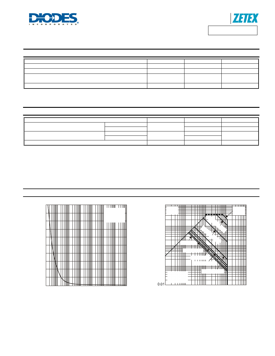
Thermal Characteristics
0
10
20
30
40
50
60
70
80
90
100
0.0001 0.001 0.01
0.1
1
10
100
1000
t , PULSE DURATION TIME (sec)
Fig. 1 Single Pulse Maximum Power Dissipation
1
P(
p
k
),
PE
AK TRA
N
SI
ENT
POW
ER
(W
)
Single Pulse
R
=205°C/W
R
(t)=R
*r(t)
T -T =P*R
(t)
θ
θ
θ
θ
JA
JA
JA
J
A
JA
0.1
1
10
100
-V
, DRAIN-SOURCE VOLTAGE (V)
DS
Fig. 2 SOA, Safe Operation Area
I
, DRA
IN CURRE
NT
(
A
)
D
0.1
1
10
100
I
(A
) @
P
=1
m
s
D
W
I
(A
) @
P
=1
00
µs
D
W
0.01
I (A) @P =10s
D
W
I (A) @ DC
D
I (A) @P =1s
D
W
I (A) @P =100ms
D
W
I (A) @P =10ms
D
W
I (A) @
P =10µs
D
W
T
= 150 C
T = 25 C
Single Pulse
J(MAX)
A
°
°
R
Limited
DS(ON)