Diodes DMP1245UFCL User Manual
Summary, Application, Features and benefits
DMP1245UFCL
Document number: DS35505 Rev. 1 - 2
1 of 7
November 2011
© Diodes Incorporated
DMP1245UFCL
ADVAN
CE I
N
F
O
RM
ATI
O
N
A Product Line of
Diodes Incorporated
12V P-CHANNEL ENHANCEMENT MODE MOSFET
Summary
V
(BR)DSS
R
DS(on)
max
I
D
max
-12V
29m
Ω @V
GS
= -4.5V
-6.6 A
45m
Ω @V
GS
= -2.5V
-5.3 A
60m
Ω @V
GS
= -1.8V
-4.6 A
100m
Ω @V
GS
= -1.5V
-3.5 A
Application
This device provides a high performance, low R
DS(ON)
P channel
MOSFETs in the thermally and space efficient X1-DFN1616-6
package. The low R
DS(ON)
of this MOSFET ensures conduction
losses are kept making it ideal for use as a:
• Battery
disconnect
switch
•
Load switch for power management functions
Features and Benefits
•
Typical off board profile of 0.5mm - ideally suited for thin
applications
•
Low R
DS(ON)
– minimizes conduction
losses
•
PCB footprint of 2.56mm
2
•
3kV ESD Protected Gate – protected against human borne
ESD
•
“Lead-Free”, RoHS Compliant (Note 1)
•
"Green" Device (Note 2)
Mechanical Data
•
Case: X1-DFN1616-6 Type E
•
Case Material: Molded Plastic, “Green” Molding Compound.
UL Flammability Classification Rating 94V-0
•
Moisture Sensitivity: Level 1 per J-STD-020
•
Lead Free Plating (NiPdAu Finish over Copper leadframe).
•
Terminals: Solderable per MIL-STD-202, Method 208
•
Weight: 0.04 grams (approximate)
Ordering Information
(Note 3)
Product
Marking
Reel size (inches)
Tape width (mm)
Quantity per reel
DMP1245UFCL-7 P5
7
8
3,000
Notes:
1. No purposefully added lead.
2. Diodes Inc’s “Green” Policy can be found on our websit
3. For packaging details, go to our website at
Marking Information
Date Code Key
Year
2011
2012
2013
2014
2015
2016
2017
Code Y
Z
A
B
C D
E
Month
Jan
Feb
Mar
Apr
May
Jun
Jul
Aug
Sep
Oct
Nov
Dec
Code 1 2 3 4 5 6 7 8 9 O N D
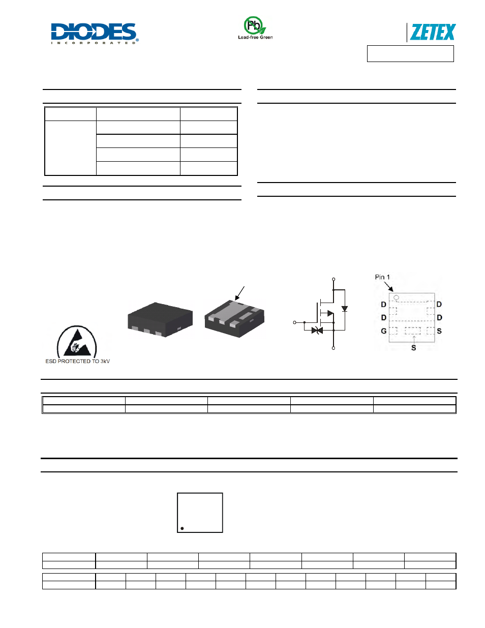
X1-DFN1616-6
Type E
Device symbol
Bottom View
Top View
Top View
Pin-Out
Pin 1
P5 = Product Type Marking Code
YM = Date Code Marking
Y = Year (ex: X = 2010)
M = Month (ex: 9 = September)
Source
Gate
Protection
Diode
Gate
Drain
P5
YM