Dmg1013t new prod uc t, Maximum ratings, Thermal characteristics – Diodes DMG1013T User Manual
Page 2: Electrical characteristics, Dmg1013t
DMG1013T
Document number: DS31784 Rev. 5 - 2
2 of 6
March 2012
© Diodes Incorporated
DMG1013T
NEW PROD
UC
T
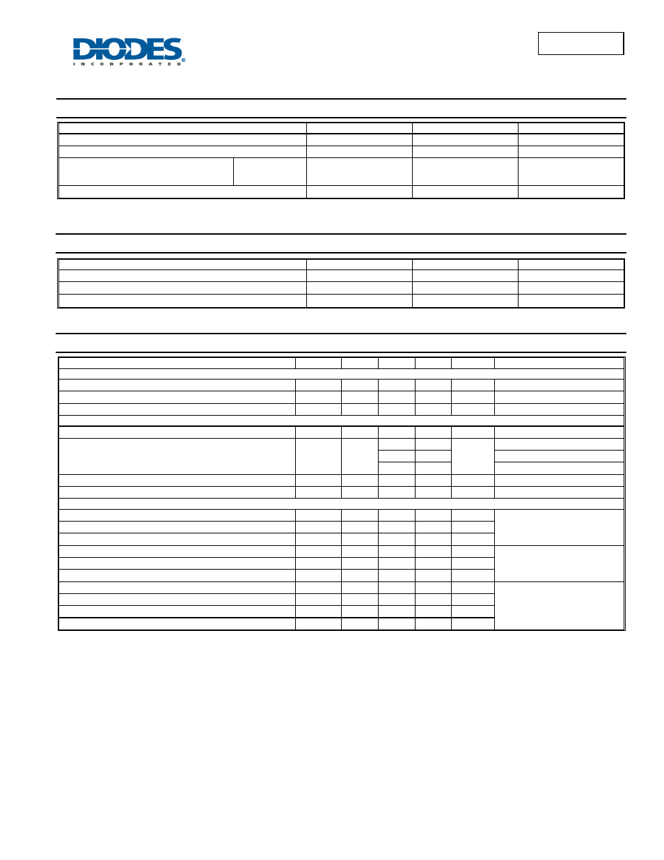
Maximum Ratings
@T
A
= 25°C unless otherwise specified
Characteristic Symbol
Value
Units
Drain-Source Voltage
V
DSS
-20 V
Gate-Source Voltage
V
GSS
±6 V
Drain Current (Note 4)
Steady
State
T
A
= 25
°C
T
A
= 85
°C
I
D
-0.46
-0.33
A
Pulsed Drain Current (Note 5)
I
DM
-6 A
Thermal Characteristics
@T
A
= 25°C unless otherwise specified
Characteristic Symbol
Value
Units
Total Power Dissipation (Note 4)
P
D
0.27 W
Thermal Resistance, Junction to Ambient (Note 4)
R
θJA
461 °C/W
Operating and Storage Temperature Range
T
J,
T
STG
-55 to +150
°C
Electrical Characteristics
@T
A
= 25°C unless otherwise specified
Characteristic
Symbol
Min
Typ
Max
Unit
Test Condition
OFF CHARACTERISTICS (Note 6)
Drain-Source Breakdown Voltage
BV
DSS
-20 - - V
V
GS
= 0V, I
D
= -250
μA
Zero Gate Voltage Drain Current T
J
= 25°C
I
DSS
- -
-100
nA
V
DS
= -20V, V
GS
= 0V
Gate-Source Leakage
I
GSS
- -
±2.0
μA
V
GS
= ±4.5V, V
DS
= 0V
ON CHARACTERISTICS (Note 6)
Gate Threshold Voltage
V
GS(th)
-0.5 - -1.0 V
V
DS
= V
GS
, I
D
= -250
μA
Static Drain-Source On-Resistance
R
DS (ON)
-
0.5 0.7
Ω
V
GS
= -4.5V, I
D
= -350mA
0.7 0.9
V
GS
= -2.5V, I
D
= -300mA
1.0 1.3
V
GS
= -1.8V, I
D
= -150mA
Forward Transfer Admittance
|Y
fs
|
- 0.9 - S
V
DS
= -10V, I
D
= -250mA
Diode Forward Voltage
V
SD
-0.8
-1.2
V
V
GS
= 0V, I
S
= -150mA
DYNAMIC CHARACTERISTICS (Note 7)
Input Capacitance
C
iss
- 59.76 -
pF
V
DS
= -16V, V
GS
= 0V,
f = 1.0MHz
Output Capacitance
C
oss
- 12.07 -
pF
Reverse Transfer Capacitance
C
rss
- 6.36 - pF
Total Gate Charge
Q
g
- 580 - pC
V
GS
= -4.5V, V
DS
= -10V,
I
D
= -250mA
Gate-Source Charge
Q
gs
- 104 - pC
Gate-Drain Charge
Q
gd
- 125 - pC
Turn-On Delay Time
t
D(on)
-
5.1
- ns
V
DD
= -10V, V
GS
= -4.5V,
R
L
= 47
Ω, R
G
= 10
Ω,
I
D
= -200mA
Turn-On Rise Time
t
r
-
8.1
- ns
Turn-Off Delay Time
t
D(off)
-
28.4
- ns
Turn-Off Fall Time
t
f
-
20.7
- ns
Notes:
4. For a device surface mounted on a minimum recommended pad layout of an FR4 PCB, in still air conditions; the device is measured when operating in
steady-state condition.
5. Same as note 4, except the device is pulsed at duty cycle of 1% for a pulse width of 10
μs.
6. Measured under pulsed conditions to minimize self-heating effect. Pulse width
≤ 300μs; duty cycle ≤ 2%
7. For design aid only, not subject to production testing.