Diodes DMN66D0LDW User Manual
Dmn66d0ldw new prod uc t, Product summary, Description
DMN66D0LDW
Document number: DS31232 Rev. 6 - 2
1 of 5
February 2014
© Diodes Incorporated
DMN66D0LDW
NEW PROD
UC
T
DUAL N-CHANNEL ENHANCEMENT MODE MOSFET
Product Summary
V
(BR)DSS
R
DS(ON)
Package
I
D
T
A
= +25°C
60V
6Ω @ V
GS
= 5V
SOT363
90mA
5Ω @ V
GS
= 10V
115mA
Description
This new generation MOSFET has been designed to minimize the
on-state resistance (R
DS(ON)
) and yet maintain superior switching
performance, making it ideal for high efficiency power management
applications.
Applications
• Load
Switch
Features and Benefits
• Dual
N-Channel
MOSFET
• Low
On-Resistance
•
Low Gate Threshold Voltage
•
Low Input Capacitance
•
Fast Switching Speed
•
Small Surface Mount Package
•
ESD Protected Gate, 1KV (HBM)
•
Lead-Free Finish; RoHS Compliant (Notes 1 & 2)
•
Halogen and Antimony Free. “Green” Device (Note 3)
•
Qualified to AEC-Q101 Standards for High Reliability
Mechanical Data
• Case:
SOT363
•
Case Material: Molded Plastic. UL Flammability Classification
Rating 94V-0
•
Moisture Sensitivity: Level 1 per J-STD-020
•
Terminals: Matte Tin Finish annealed over Alloy 42 leadframe
(Lead Free Plating). Solderable per MIL-STD-202, Method 208
•
Terminal Connections: See Diagram
•
Weight: 0.006 grams (approximate)
Ordering Information
(Note 4)
Part Number
Case
Packaging
DMN66D0LDW
-7
SOT363
3,000/Tape & Reel
Notes:
1. No purposely added lead. Fully EU Directive 2002/95/EC (RoHS) & 2011/65/EU (RoHS 2) compliant.
2. S more information about Diodes Incorporated’s definitions of Halogen- and Antimony-free, "Green"
and Lead-free.
3. Halogen- and Antimony-free "Green” products are defined as those which contain <900ppm bromine, <900ppm chlorine (<1500ppm total Br + Cl) and
<1000ppm antimony compounds.
4. For packaging details, go to our website at
Marking Information
Date Code Key
Year
2007
2008
2009
2010 2011 2012 2013 2014 2015 2016 2017
Code
U V W X Y Z A B C D E
Month
Jan
Feb
Mar
Apr
May
Jun
Jul
Aug
Sep
Oct
Nov
Dec
Code
1 2 3 4 5 6 7 8 9 O N D
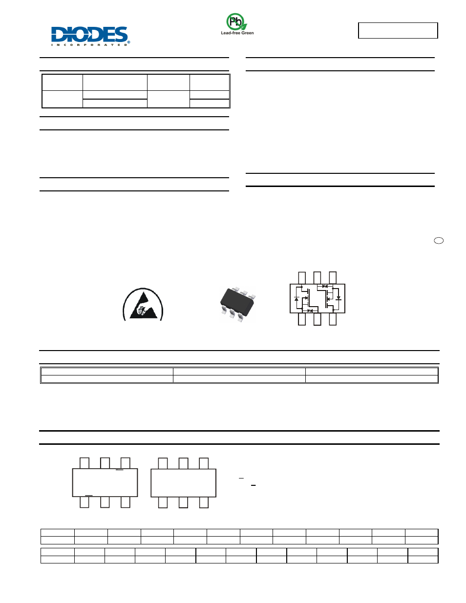
SOT363
Top View
Top View
Internal Schematic
S
1
D
1
D
2
S
2
G
1
G
2
MN1
MN1
YM
YM
ESD PROTECTED TO 1kV
MN1= Product Type Marking Code
YM = Date Code Marking for SAT (Shanghai Assembly/ Test site)
YM = Date Code Marking for CAT (Chengdu Assembly/ Test site)
Y or Y = Year (ex: A = 2013)
M = Month (ex: 9 = September)
MN1
MN1
YM
YM
e3