Electrical characteristics, Dms3012sfg – Diodes DMS3012SFG User Manual
Page 4
POWERDI is a registered trademark of Diodes Incorporated.
DMS3012SFG
Document number: DS35441 Rev. 7 - 2
4 of 8
October 2012
© Diodes Incorporated
DMS3012SFG
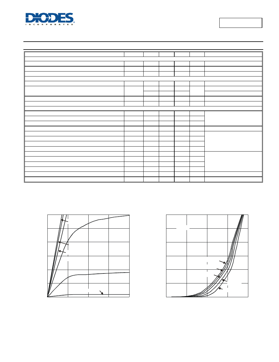
Electrical Characteristics
(@T
A
= +25°C, unless otherwise specified.)
Characteristic
Symbol
Min
Typ
Max
Unit
Test Condition
OFF CHARACTERISTICS (Note 8)
Drain-Source Breakdown Voltage
BV
DSS
30 — — V
V
GS
= 0V, I
D
= 250
μA
Zero Gate Voltage Drain Current
I
DSS
—
—
100
μA
V
DS
= 30V, V
GS
= 0V
Gate-Source Leakage
I
GSS
—
—
±100 nA
V
GS
= ±20V, V
DS
= 0V
ON CHARACTERISTICS (Note 8)
Gate Threshold Voltage
V
GS(th)
1.0 1.5 2.5 V
V
DS
= V
GS
, I
D
= 250
μA
Static Drain-Source On-Resistance
R
DS (ON)
—
7.3 10
m
Ω
V
GS
= 10V, I
D
= 13.5A
—
10 15
V
GS
= 4.5V, I
D
= 11A
Forward Transfer Admittance
|Y
fs
|
—
30 — S
V
DS
= 5V, I
D
= 10.0A
Diode Forward Voltage
V
SD
—
0.45 0.55 V V
GS
= 0V, I
S
= 1A
DYNAMIC CHARACTERISTICS (Note 9)
Input Capacitance
C
iss
—
1296 4310 pF
V
DS
= 15V, V
GS
= 0V,
f = 1.0MHz
Output Capacitance
C
oss
—
415 —
pF
Reverse Transfer Capacitance
C
rss
—
204 —
pF
Gate Resistance
R
g
0.26 1.6 2.6
Ω
V
DS
= 0V, V
GS
= 0V, f = 1MHz
Total Gate Charge V
GS
= 4.5V
Q
g
—
14.7 —
nC
V
DS
= 15V, V
GS
= 10V, I
D
= 13.5A
Total Gate Charge V
GS
= 10V
Q
g
—
31.6 —
nC
Gate-Source Charge
Q
gs
—
3.5 —
nC
Gate-Drain Charge
Q
gd
—
5.0 —
nC
Turn-On Delay Time
t
D(on)
—
15.8 —
ns
V
GS
= 10V, V
DS
= 15V,
R
G
= 3
Ω, I
D
= 8.8A
Turn-On Rise Time
t
r
—
27.8 —
ns
Turn-Off Delay Time
t
D(off)
—
29.7 —
ns
Turn-Off Fall Time
t
f
—
13.6 —
ns
Reverse Recovery Time
t
rr
—
13.1 —
ns
I
F
= 13.5A, di/dt = 100A/
μs
Reverse Recovery Charge
Q
rr
—
4.3 —
nC
I
F
= 13.5A, di/dt = 100A/
μs
Notes:
8. Short duration pulse test used to minimize self-heating effect.
9. Guaranteed by design. Not subject to product testing.
0
0.5
1
1.5
2
Fig. 4 Typical Output Characteristic
V
, DRAIN-SOURCE VOLTAGE (V)
DS
0
10
15
20
25
30
I,
D
R
AI
N
C
U
R
R
EN
T
(A)
D
5
V
= 2.0V
GS
V
= 2.5V
GS
V
= 3.0V
GS
V
= 3.5V
GS
V
= 4.5V
GS
V
= 4.0V
GS
1.0
1.5
2.0
2.5
3.0
0
5
10
15
20
25
30
I,
D
R
AI
N
C
U
R
R
EN
T
(A
)
D
Fig. 5 Typical Transfer Characteristic
V
, GATE-SOURCE VOLTAGE (V)
GS
V
= 85°C
GS
V
= 125°C
GS
V
= 25°C
GS
V
= -55°C
GS
V
= 150°C
GS
V
= 5V
DS